Thursday, March 25, 2021

100W RMS Audio Amplifier using TDA7294 IC + PCB

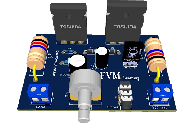
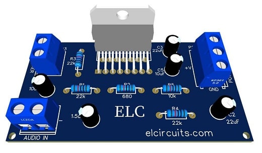
Fig. 1 - Printed Circuit Board Amplifier 100W with TDA7294


We'll assemble an excellent power amplifier, with excellent sound quality, with 100W RMS output power, with symmetrical power supply. The circuit has a wide range in the supply voltage, and we will be providing the printed circuit board for you to download.

Integrated Circuit

The TDA7294 is an Integrated Circuit with Class AB audio output, it has its Multiwatt encapsulation. It was specifically designed for high quality sound applications, such as: home micro-systems, guitar cubes, high-end televisions. 

Thanks to the wide voltage range and the high current capacity, it's able to provide the highest power in loads of 8 ohms or 4 ohms, even with low supply voltage input, with high voltage rejection circuit.

The built-in locking function with activation delay simplifies remote operation, avoiding noisy changes when pressing the On/Off button.

Characteristics

  • Wide range of supply voltage (± 10V to ± 40V)
  • DMOS output amplification step
  • High Output Power (Musical 100W)
  • Mute and Stand-by functions
  • Very low harmonic distortion
  • Short circuit protection
  • Thermal protection with automatic shutdown

The layout of the schematic diagram is just below in Figure 2, for which we have the entire configuration of the amplifier with TDA7294.
Fig. 2 - Schematic diagram 100W RMS Audio Amplifier IC TDA7294

List of materials

  • U1 .................. Integrated Circuit TDA7294
  • R1, R3, R4 .... Resistor 22K (red, red, orange, gold)
  • R2 ................. Resistor 680Ω (blue, gray, brown, gold)
  • R5 ................. 10K resistor (brown, black, orange, gold)
  • C1 .................. Electrolytic capacitor 1.5μF - 35V
  • C2, C3 ........... Electrolytic capacitor 22μF - 63V
  • C4, C5 ........... Electrolytic capacitor 10μF - 63V
  • P1, P3............. 2-Pin Card-to-Cable Connector
  • P2 .................. 3-Pin Card-to-Cable Connector
  • Others ............ Printed Circuit Board, tin, wire, etc.

Power supply

The power supply must be at least 5 AmperesSymmetrical, with good filtration, with a minimum voltage of 10 Volts and a maximum of 40 Volts

Knowing that using the minimum voltage, you will not reach the maximum power of the amplifier, because it needs a higher voltage to supply the declared power.

In this amplifier model, is used a Symmetric Power Supply type, that is; power [+ VCC GND | -VCC].

Download

We are making available for download the necessary materials for those who want to assemble with the PCB - Printed Circuit Board, the files in PNG, PDF and GERBER files, for those who want to send for printing.

Direct link to download

Click in the link below to download the Files: PCB Layout, PDF, GERBER

If you have any questions, suggestions or corrections, please leave them in the comments and we will answer them soon.

Subscribe to our blog!!! Click here - elcircuits.com!!!

My Best Regards!!!

Sunday, March 21, 2021

Adjustable Power Supply 1.25v to 57V, 6 Amps using TIP36C + LM317HV + PCB

The LM317HV is an adjustable 3-terminal positive voltage regulator capable of supplying 1.5 A or more currents over a 1.25V to 57V output voltage range. It requires only two external resistors to set the output voltage. The LM317HV is packaged in standard transistor packages that are easily mounted and handled.

However, the LM317HV supports high voltage, but the current is still low, only 1.5A, our circuit, we are increasing a drive circuit to increase the current we need to 6 Amps, with three TIP36C transistors, which provides an adjustable output voltage between 1.25v to 57 volts, with a current of 6 Amps, which is enough for a bench power supply.

The Circuit

The schematic electrical diagram, which follows in Figure 2 below, it's very simple, first one, we have the voltage input that comes through connector J1, which enters through resistor R1, that as long as there is no current greater than the one calculated, there is no drop of voltage in R1, more if the current increases, there will be a voltage drop of approximately 0.6V, which will cause the transistors to saturate, causing the current to pass through the power transistors.

The capacitor C1 has the objective of attenuating the interference of the ripples and their stability. Capacitor C2 has the function of eliminating high interference, and capacitor C3 has the function of constancy to decrease the ripple and stability of the power supply. 

P1, is a 5K analog potentiometer, if you don’t have 5K you can put 4.7K, which is more commercial, the diodes D1 and D2 are to avoid reverse voltage over the Integrated Circuit U1, and in the transistors, resistors R3, R4 and R5, are impact resistors, which attenuate the difference between the transistors and prevent one from working more than the other.
Fig. 2- Adjustable Power Supply Schematic LM317HV + TIP36

Components list

  • U1…………….... LM317HV – Integrated circuit, voltage regulator
  • Q1,Q2,Q3 ...…... TIP46C Power Transistor
  • D1, D2 ………....1N4007- Silicon rectifier diodes
  • C1 ……………... 470 uF – 65V – Electrolytic capacitor
  • C2 ……………... 100 nF  Ceramic capacitor
  • C3 ……………... 2200 uF – 65V – Electrolytic capacitor
  • R1 ……………... 10 ohms – 1W – brown, black, black, gold
  • R2 ……………... 2K ohms – 1/4 W – red, black, orange, gold
  • R3, R4, R5 .….... 0.22 ohms – 5W – red, red, silver, gold
  • R6 ……………... 220 ohms – 1/4W – red, red, brown, gold
  • P1 ……………... 5 K ohms or 4,7 k ohms – Linear potentiometer
  • J1, J2 …….……. Kre Block Terminal Terminal 2-Way Double Connector
  • Others ............… Printed Circuit Board, tin, wire, etc.

We are offering to Download the link with the printed circuit board printing files, they are; Gerber, PDF layout, PNG, all the files with a direct link to Mega.

Direct link to download

Click in the link below to download the Files: PCB Layout, PDF, GERBER

If you have any questions, suggestions or corrections, please leave them in the comments and we will answer them soon.

Subscribe to our blog!!! Click here - elcircuits.com!!!

My Best Regards!!!

Saturday, March 20, 2021

100W RMS Power Amplifier using 2 NPN 2SC5200 Output Transistors + PCB

Fig. 1 - 100W RMS Power Amplifier using 2 NPN 2SC5200 Output Transistors + PCB

For Portuguese version, click here!

We usually have amplifiers with complementary outputs on most amplifier designs, and in a vast majority of amplifiers, it's quite normal to use the complementary NPN 2SC5200 transistors in conjunction with the PNP 2SA1943.

This type of amplifier is very common and good quality, because these transistors are specific for high fidelity amplification.

You might also be interested in:

We'll build an amplifier circuit that uses the same concepts as two output transistors, but we will use two NPN 2SA5200 output transistors. Which is very interesting for those who like to test other types of transistors to evaluate the quality, distortions, powers. Etc.

The schematic diagram is in Figure 2 below, it is a simple amplifier, it has a satisfactory quality.

Fig. 2 - 100W RMS Power Amplifier with 2 NSC 2SC5200 Transistors at Output

Power Supply

The power supply consists of a symmetrical transformer 32V - 0 - 32V center tape, with a current of 5 Amperes, a lower current, up to 3 Amperes minimum, can be used, which will play without any problems.

Nothing prevents you from using a higher or lower voltage, as this amplifier has a tolerance for the supply voltage, and can normally play “with small attenuation in the output power” with voltages ranging from 18V to 55V without too many difficulties.

It also has great stability, and we can use, if you have, a SMPS power supply, and this is clear with Center-Tape, that is to say a power supply with central socket.

Component List

  • Q1, Q2 ............... Transistor A733
  • Q3, Q4 ............... TIP41C transistor
  • Q5 ...................... TIP42C transistor
  • Q6, Q7 ............... 2SC5200 Power Transistor

  • D1, D2, D3 ........ Diode 1N4007

  • C1 ....................... 0.47uF Polyester capacitor 
  • C2, C4, C5 .......... 47uF - 63V electrolytic capacitor 
  • C3 ....................... 100nF ceramic / polyester capacitor 
  • C6 ....................... 150pF ceramic / polyester capacitor 
  • C7, C8 ................ 1nF ceramic / polyester capacitor

  • R1 ....................... 22k ohms resistor (red, red, orange, gold)
  • R2 ....................... 15k ohms resistor (brown, green, orange, gold)
  • R3, R7 ................. 680 ohms resistor (blue, gray, brown, gold)
  • R4 ....................... 33 ohms resistor (orange, orange, black, gold)
  • R5 ....................... 560 ohms - 1W resistor (green, blue, brown, gold)
  • R6 ....................... 56k ohms resistor (green, blue, orange, gold)
  • R8, R9 ................ 4.7k ohms resistor (yellow, violet, red, gold)
  • R10 ..................... 10 ohm resistor - (brown, black, black. gold)
  • R11 ..................... 120 ohms - 1W resistor (brown, red, brown, gold)
  • R12, R13 ............ 100 ohms - 1W resistor (brown, black, brown, gold)
  • R14, R15 ............ 0.47 ohms - 5W resistor (yellow, violet, silver, gold)

  • Others ................. PCB, Heat Sink, Loudspeaker, Wires, Solders, Etc.

For those who want to download materials such as the schematic diagram in PDF, PCB Layout,  GERBER and JPG, we are providing a direct link to download all the material.

Direct link to download

Click in the link below to download the Files: PCB Layout, PDF, GERBER, JPG

If you have any questions, suggestions or corrections, please leave them in the comments and we will answer them soon.

Subscribe to our blog!!! Click here - elcircuits.com!!!

My Best Regards!!!


Friday, March 12, 2021

Simple 3 Transistors Power Amplifier push a 600W RMS Subwoofer + PCB

Fig. 1 - Simple 3 Transistors Power Amplifier PCB


This is a simple amplifier that uses only 3 transistors, and has the ability to push a 600W RMS Subwoofer speaker with great mastery.

The circuit is quite simple, and easy to assemble, we took this circuit from our Brazilian partner FVM Learning, and this is their direct link www.fvml.com.

This mini amplifier was tested in two stages, one with 24V, with a non-symmetrical power supply, and in 30V also with non-symmetrical power, the result you can watch in the original video at the end of this post.

You might also be interested in:

The Amplifier Circuit

The amplifier circuit is very simple to be arranged in figure 2 just below, it is divided into two stages: 

  • The first stage is the pre-amplification and at the same time used as a drive to boost the output stage. It is formed by a transistor medium power the BD139, which supports a voltage of up to 80V and a current of 1.5A with 12.5 W of power, according to the Datasheet of the same.

  • The second is the power stage, which is formed by the complementary transistors NPN - 2SC5200 and the PNP - 2SA1943 transistor, with 100W of power and high fidelity, whose collector current supported is 15 Amps.
Fig. 2 - Simple 3 transistors Power Amplifier schematic diagram

Note

Place the power transistors in a heat sink, especially if you are going to apply a voltage greater than 20V and use the amplifier continuously, they will heat up.

Component List

  • T1 ---------- NPN 2SC5200 Power complementary transistor
  • T2 ---------- PNP Complementary Power Transistor 2SA1943
  • T3 ---------- NPN BD139 transistor

  • D1, D2 ----- Diode 1N4007

  • C1 ---------- Electrolytic capacitor 2.200uF - 63V
  • C2 ---------- Electrolytic capacitor 4.7uF - 25V

  • R1, R2 ----- Resistor 0.22 ohms - 5W - (red, red, silver)
  • R3 ---------- Resistor 1k ohms - (brown, black, red)
  • R4 ---------- Resistor 100k ohms - (brown, black, yellow)

  • P1 ---------- 10K ohm potentiometer

  • Others ----- Wires, Welds and Etc.

Watch the original video of the FVML channel of the tests, and the assembly step by step, and be surprised !!!!


We are offering to download the link with the printed circuit board printing files, they are; Gerber, PDF layout, PNG, all the files with a direct link to Mega.

Direct link to download

Click in the link below to download the Files: PCB Layout, PDF, GERBER
Click Here!!!

If you have any questions, suggestions or corrections, please leave them in the comments and we will answer them soon.

Subscribe to our blog!!! Click here - elcircuits.com!!!

My Best Regards!!!

Friday, February 19, 2021

200W RMS Stereo Power Amplifier using STK4231II IC + PCB

Fig. 1 - PCB 200W RMS Stereo Power Amplifier IC STK4231II


This audio amplifier circuit is a HI-FI two-channel 100w OCL High Power Stereo Audio Amplifier based on the STK4231II IC.

STK4231 is a Thick film hybrid IC two-channel  100W min AF Power Amp, manufactured by SANYO ELECTRIC CO. LTD JAPAN. The STK4221II IC is a dual high power amplifier chip, preferably suited for compact high power audio applications, it provides 2 channel high power best quality audio output of 100W RMS at both channel at 8Ω speaker.


You might also be interested in:

Features

The STK4201II series are pin-compatible in the range output of 60W to 100W, are 22 pin SIP (Single Inline Package) IC with a special case designing for operation at more heat dissipation to generally reduce external heat sink. 

But use a heat sink for protection. This IC is generally used in the home microsystem, car audio. The real IC image is shown below in Figure 2.

Fig. 2 - Pinout of IC STK4231II

Figure 3 below, show the schematic circuit diagram 100W + 100W RMS Stereo Power Audio Amplifier to be followed, with the arrangement of the components and their configurations.

Fig. 3 - Schematic 200W Stereo power amplifier IC STK4231II

Components List

  • U1................................. STK4231II – Audio Amplifier Integrated Circuit
  • R1, R2, R8 ................... 1K ohms - 1/8 W – brown, black, red
  • R3, R4, R12, R16 ........ 56K ohms - 1/8 W – green, blue, orange
  • R5, R6 .......................... 1K ohms - 1W – brown, black, red
  • R7 ................................. 100 ohms - 1/8 W – brown, brown, black
  • R9, R14 ........................ 4.7K ohms - 1/8 W – yellow, violet, red
  • R10, R18 ...................... 4.7K ohms - 1W – yellow, violet, red
  • R11, R15 ...................... 0.22 ohms - 5W – red, red, silver, gold , black
  • R13, R17 ...................... 560 ohms - 1/8 W – green, blue, brown
  • R19, R20, R21, R22 ..... 4.7 ohms - 18W – yellow, violet, gold
  • R10 ............................... 4.7K ohms - 1W – yellow, violet, red
  • C1, C2 .............................. 470pF – Polyester or Ceramic Capacitor
  • C3, C4 .............................. 2.2uF – Electrolytic Capacitor
  • C5, C6, C7, C8, 9, C10 .... 10uF - 63V – Electrolytic Capacitor
  • C11, C12 .......................... 47 uF - 63V – Electrolytic Capacitor
  • C13, C14 ......................... 100 nF – Polyester or Ceramic Capacitor
  • L1, L2 .............................. 3uH inductor
  • J1, J2 ................................ Kre Block Terminal Terminal 3-Way Triple Connector
  • J1, J2 ................................ Kre Block Terminal Terminal 2-Way Double Connector
  • Others .............................. Printed Circuit Board, tin, wire, etc.

Specified Transformer Power Supply

The power transformer must have a Dual Supply Capacity and  5 Amperes minimal current, this circuit is powered by a constant-voltage Dual Power Supply (+50V, 0V, -50V) CC,  for the correct operation. 

The power supply is the same as the one in Figure 4, available on the FVML website which is our partner, the difference is that the transformer is 35V AC, which after filtering will be approximately 50V DC.

Clicking in image below, you will be directed to the FVML website, which even has the calculations to understand it better and the printed circuit board files with GERBER files to download.
Fig. 4 Schematic Power Supply, click to download free the Gerber files


We are offering to download the link with the printed circuit board printing files, they are; Gerber, PDF layout, PNG, all the files with a direct link to Mega.

Direct link to download

Click in the link below to download the Files: PCB Layout, PDF, GERBER

If you have any questions, suggestions or corrections, please leave them in the comments and we will answer them soon.

Subscribe to our blog!!! Click here - elcircuits.com!!!

My Best Regards!!!

Saturday, February 6, 2021

Adjustable Power Supply 1.25v to 33V, 3 Amps using LM350 + PCB

Fig. 1 - PCB Power Supply LM350

Nowadays it is very important and necessary to have a bench power supply to test ours; projects, electronic circuits, to maintain equipment, among others. However, this power supply must have at least a voltage adjustment control, and at least a short circuit protection.

And this is the proposal of this circuit, a simple and very effective circuit, with protection against short circuit, and that brings in its output an adjustable voltage between, 1.25v to 33 volts, with a current of 3 Amps, which is enough for most of the projects, and still, this PS has protection circuit against short circuit and over-temperature protection.

You may be interested in: 

The LM350 Integrated Circuit

The LM350 IC is an adjustable three-pin positive voltage regulator capable of delivering 3.0 Amperes in an output voltage range of 1.2 V to 33 V. This voltage regulator is exceptionally easy to use and requires only two external resistors to adjust the output voltage.
Besides:

  • Internal Current Limiting
  • Thermal shutdown
  • Secure Area Compensation

What do the LM350 integrated circuit, an essentially explosion-proof component.
The LM350 serves a wide variety of applications:

  • Static Voltage Regulator for digital circuits
  • Stable Current Regulator
  • Variable Current Regulator

This device also does an especially simple adjustable switching regulator, a programmable output regulator, or connecting a fixed resistor between the setting and the output, the LM350 can be used as a precision current regulator:

  • Guaranteed 3.0 The output current
  • Adjustable output between 1.2 V and 33 V
  • Load Regulation Normally 0.1%
  • Line Regulation Normally 0.005% / V
  • Internal thermal overload protection
  • Temperature Short-Circuit Internal Current Limiting Current
  • Compensation of the safe area of the output transistor
  • Floating Operation for High Voltage Applications
  • Standard 3-way Transistor Package
  • Eliminates Socks Many Back Fix

The Circuit

The electric schematic diagram, it follows in Figure 2 below, is quite simple, first, we have the rectifier diode bridge KBL610 that is a bridge of 6 Amperes to 1000 Volts, however, you can use anyone that you have and that is above 4 Amperes over 50 Volts.

Diodes D2 and D3 are for the protection of the IC LM350, against short circuits, because when we start the Power Supply, and the capacitor C3 is totally discharged, and it becomes as a short-circuit for the IC.

The C1 capacitor is to attenuate the ripples interference and stability of the same. The C2 capacitor has the function of constancy to decrease Ripple, and stability of the power supply. 

P1, is an analog potentiometer of 5K, if you don’t have the 5K you can put a 4.7K, which is more commercial. T1 is a transformer of at least 3 Amperes, with input according to your local network, which can be 220v or 110v depending on your region, and the transformer secondary is 25 Vac for the output of 33 Vdc.

Fig. 2- Adjustable Power Supply Schematic LM350

So you want to do a more powerful adjustable power supply, for example with 6 Amps, we have this adjustable module post in the link below:

Components List

  • U1 ........... LM350T – Integrated circuit, voltage regulator
  • D1 ........... KBL610 Silicon Rectifier Diode Bridge
  • D2, D3 .... 1N4007- Silicon rectifier diodes
  • C2 ........... 4700 uF – 50V – Electrolytic capacitor
  • C3 ........... 100 uF – 50V – Electrolytic capacitor
  • R1 ........... 220 ohms – ½ W – red, red, brown
  • T1 ........... Transformer 25 V with a minimum current of 3A
  • RP1 ......... 5 K ohms or 4,7 k ohms – Linear potentiometer
  • P1, P2 ...... Kre Block Terminal Terminal 2-Way Double Connector
  • Others .... Printed Circuit Board, tin, wire, etc.

We are offering to Download the link with the printed circuit board printing files, they are; Gerber, PDF layout, PNG, all the files with a direct link to Mega.

Direct link to download

Click in the link below to download the Files: PCB Layout, PDF, GERBER

If you have any questions, suggestions or corrections, please leave them in the comments and we will answer them soon.

Subscribe to our blog!!! Click here - elcircuits.com!!!

My Best Regards!!!