Thursday, April 8, 2021

Adjustable Power Supply 1.2 to 37V High Current 20A using LM317 and TIP35C + PCB

Fig. 1 - PCB Adjustable Power Supply 1.2V to 37V - 20A


For Portuguese version, click here!

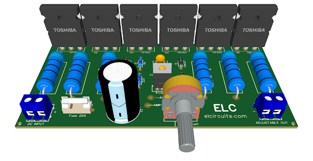
This is a High Current Variable Power Supply circuit, which works smoothly *With 20 Amps. And we will use the old, wonderful, and well-known LM317, which is an Integrated Circuit regulating positive variable voltage with a range of 1.25 to 37V, and 1.5 Amps.  

We obtained this circuit from our partner FVM Learning, which made it available to us, we made few changes, such as increasing the transistors that they speak of in the Original Post, and we made the PCB that was not available until now, the rest is exactly the same.

To make an appropriate Power Supply, it is necessary to have a current well greater than 1.5A, so that’s where the power transistors come in, they’re going to increase the current without varying the voltage.

Because this variation function is up to the LM317, and the current factor is up to the transistors that in this circuit we’re going to use TIP35C.

Circuit Operation

The LM317 is a variable positive voltage regulator, which is responsible for varying the output voltage and delivering the base of the power transistors to this variable voltage. 

Which together with the other transistors form a high current booster, and which depending on the amount of transistor and the sum of the currents of each transistor, we form a high current variable power supply.

The voltage that comes from the power supply enters directly into the TIP35C collector, and is controlled by varying the input voltage at the base. 

And in turn the voltage that will come out of the emitter, will be directly related to the control of the output voltage of the LM317, it is necessary to use a heat sink, as this holding energy is converted into heat.

The TIP35C is a High Power Mospec transistor, with a 25A continuous collector current capacity, thus making it the perfect transistor for this project.

* It is worth remembering that this transistor has a total power of 125W, that means that following the Ohms Law, the current was calculated by the manufacturer for this transistor at 5V, let's check:

Ohms Law Formula: P = V * I

P = Power: V = Voltage: I = Current:
I = P / V ==> I = 125/5 ==> I = 25A

In our case where the power supply will go up to 37V, we can consider that:
I = P / V ==> I = 125/37 ==> I = 3.38A

Did you see the difference? We put two transistors for this work, but if you are going to use this source continuously with the maximum voltage and total current, you will need to add two more pairs in this circuit. 

We can use this power supply with these parameters; Voltage, Current, maximum, but for continuous use, it will overheat the transistors and burn.

The TIP35C has 100V of Vce and Vbe, Emitter Collector Voltage, and Base Collector Voltage. Remember this, these settings refer to the TIP35C, there are other variants such as: TIP35 = 40V, TIP35A = 60V, TIP35B = 80V and TIP35C = 100V, so for this project you can use the TIP35C for greater efficiency.

The Adjustable Power Supply schematic diagram is shown in Figure 2, which shows the arrangement of the components and their connections to proceed with the assembly, which in the general context, is quite simple to assemble, and demonstrates a great effectiveness.

Fig. 2 - Schematic Diagram Adjustable Circuit - 1.25V ~ 37V, 20A CI LM317 and TIP35C

Components List

  • U1 ............................ LM317 voltage regulator integrated circuit
  • Q1 to Q6 .................. TIP35C Power Transistor
  • D1, D2, D3, D4 ....... 1N4007 Silicon rectifier diodes 
  • C1 ............................ 4700uF - 63V Electrolytic capacitor 
  • C2, C3 ..................... 0.1uF Ceramic / Polyester Capacitor 
  • R1 ............................ 220 ohms 1 / 4W Resistor - (red, red, brown, gold)
  • R2 ............................ 10K ohms - 1/4 W Resistor - (brown, black, orange, gold)
  • R3 to R8 .................. 0.22 ohms - 5W Resistor - (red, red, silver, gold)
  • P1 ............................ 5k ohms Potentiometer 
  • J1, J2 ....................... PCB Terminal Blocks - EK500V-XXP 20A - or equivalent
  • F1 ............................ PCB Fuse Clip Cartridge 250V 30A With Fuse 20A
  • Others ..................... Wires, Welds, Posts, PCB, Etc.

For those who want to download materials such as the schematic diagram in PDF, PCB Layout,  GERBER and JPG, we are providing a direct link to download all the material.

Direct link to download

Click in the link  to download the Files: PCB Layout, PDF, GERBER, JPG

If you have any questions, suggestions or corrections, please leave them in the comments and we will answer them soon.

Subscribe to our blog!!! Click here - elcircuits.com!!!

My Best Regards!!!

Wednesday, April 7, 2021

320W Power Audio Amplifier, Powered with 14.4V - 2Ω using TDA7560 IC + PCB

Fig. 1 - 320W Power Audio Amplifier - IC TDA7560


This is a simple high power amplifier circuit, with 320W divided into 4 outputs with 2Ω. This amplifier is capable of providing 50 Watts of power per channel, totaling 200W of sound power. 

But, what title does it say is 320W? That's right, the amplifier circuit with TDA7560 for which it is the base of this amplifier, was designed to provide a maximum power of 80 Watts per channel with a load of 2Ω powered by 14.4V.

Which opens up great possibilities for those who do not usually use symmetrical power supply, and you can also use this circuit as an amplifier in your car.

Since the connected car provides approximately 14.4V that serves to charge the battery, and without taking into account that this circuit may also be being powered directly by 12V, which would be when the car is off.

Output Power Settings:

For 4Ω load

VS = 13.2V - THD 10% - 4 x 25 Watts
VS = 13.2V - THD 1% - 4 x 19 Watts
VS = 14.4V - THD 10% - 4 x 30 Watts
VS = 14.4V - THD 1% - 4 x 23 Watts

For 2Ω load

VS = 13.2V - THD 10% - 4 x 45 Watts
VS = 13.2V - THD 1% - 4 x 34 Watts
VS = 14.4V - THD 10% - 4 x 55 Watts
VS = 14.4V - THD 1% - 4 x 43 Watts

Maximum Power THD> 10%

VS = 14.4V - 4Ω - 4 x 50 Watts
VS = 14.4V - 2Ω - 4 x 80 Watts

Characteristics

  • Hi-Fi Distortion Class
  • Low output noise
  • St-by function
  • Mute function
  • Auto Mute in min. Supply voltage detection
  • Supply voltage range from 8 to 18Volts
  • Low external component account:
  • Internally fixed gain (26db)
  • No external compensation
  • Without Bootstrap Enablers
  • 0.35A onboard pre-driver

Standby and Mute

The Standby and Mute installations are both compatible with CMOS, if you do not want to use a direct connection with the respective Vs pins.

You can use standard low power transistors to drive the Mute and Stand-By pins if you do not want to use the ports CMOS or even use microprocessors.

The R-C set should always be used to smooth the transitions to avoid audible transient noise. In Stand-By mode, the time constant to be assigned to achieve a transition practically free of pop-ups must be slower than 2.5V / ms.

In Figure 2 below, we have the schematic diagram of the Audio Amplifier with 320W Power, powered with 14.4V with IC TDA7560, as we can see, it is a very simple circuit, compared to its insight, so small.

However, quite powerful, and this is great because it makes assembly a lot easier for those who do not have great experiences with electronics and also wants to participate in this excellent and incredible world of electronics.
Fig. 2 - Audio Amplifier with 320W - Powered with 14.4V with CI TDA7560

The power supply must provide a current of at least 7 Amperes. It is important to remember that the maximum supply voltage allowed by this IC is 18 Volts, if we exceed this supply voltage we can burn the Integrated Circuit.

Components List

  • CI 1 ................................ TDA7560 Integrated Circuit
  • R1 .................................. 10KΩ Resistor (brown, black, orange, gold)
  • R2 .................................. 47 KΩ Resistor (yellow, violet, orange, gold)
  • C1, C2 ........................... 1μF Ceramic capacitor / polyester
  • C3, C4, C5, C6, C9 ....... 0.1μF Ceramic / polyester capacitor 
  • C7 .................................. 470nF Ceramic / polyester capacitor 
  • C8 .................................. 47μF - 25V Electrolytic capacitor 
  • C10 ................................ 2.200μF - 25VElectrolytic capacitor 
  • CN 1, 2, 4, 5, 6, 7, 8 ...... 2-Pin PCB Terminal Blocks - EK500V-XXP
  • CN 3 .............................. 5-Pin Card-to-Cable Connector
  • Others ............................ Printed Circuit Board, tin, wire, etc.
The PCB - Printed Circuit Board, has its dimensions of; 83.439mm width by 58.166mm depth, and, We are making available for Download the necessary materials for those who want to assemble with PCB, the files in PNG, PDF and GERBER files for those who want to send for printing.

Download:

Direct Link: PNG, PDF, GERBER files

This post is an authorized copy of our partner www.fvml.com.br. For those who want to follow step by step the assembly of this amplifier and the sound tests, you can access the video in Portuguese on the FVML Youtube channel by accessing below.

If you have any questions, suggestions or corrections, please leave them in the comments, and we will answer them soon.

Subscribe to our blog!!! Click here - elcircuits.com!!!

My Best Regards!!!

Thursday, April 1, 2021

50W RMS Audio Amplifier with IRF530 and IRF9530 Mosfet + PCB

Fig. 1 - PCB 50W Audio Amplifier

For Portuguese version, click here!

This circuit amplifier is very simple to building, however, although simple, it has an excellent audio quality, and with just two output transistors, it reaches a sound power of 50W RMS under load of 8 ohms, which is enough for a great home sound system, or for speakers for musical instruments ... the possibilities are endless.

The first stage of the amplifier is a differential amplifier based on the transistors Q1 and Q2. Capacitor C2 is the input DC decouple, R1 limits the input current and capacitor C1 deflects unwanted high frequencies.

You might also be interested in:

The second stage is the drive stage composed of the transistor Q3 BC546, which supplies the output power stage, and the transistor Q4 is the bias regulating transistor, which, through the PR1 trimpot, adjusts the quiescent current in the transistors.

The output stage is a complementary push-pull stage based on the IRF530 and IRF9530 MOSFETs. The output is coupled to the speaker using the L1 inductor

The network composed in series by hairs, resistor R14 and capacitor C5, is intended to reduce output noise. And Capacitors C6 and C7 are power supply voltage filters. 

For coil L1: Wrap 12 turns of enameled copper wire in a 1cm diameter without core.

A Heatsink is required for MOSFETs. That should have the average dimensions of 8x4x4 inches will already work without problems.

You can check the schematic diagram in Figure 2 below.

Fig. 2 - 50 Watt Amplifier Circuit Diagram

Power Supply

The power supply consists of a symmetrical transformer 35Vcc - 0 - 35V center tape, with a current of 3 Amperes, a lower current, up to 2 Amperes minimum, can be used, which will play without any problems. 

Nothing prevents you from using a higher or lower voltage, as this amplifier has a tolerance for the supply voltage, and can normally play "with small attenuations in the output power" with voltages ranging from 27V to 40V without too many problems.

It also has great stability and we can use, if you have, a SMPS power supply, and this is clear with Center-Tape, that is to say a power supply with central socket.

Component List

  • Q1, Q2 ................ 2N3906 Transistor (or BC558, A733)
  • Q3, Q4 ................ 2N3904 Transistor (or BC548)
  • Q5 ....................... IRF9530P Mosfet P Transistor
  • Q6 ....................... IRF530P Mosfet N Transistor

  • D1 ....................... 1N4007 Diode 

  • C1 ....................... 220pF ceramic / polyester capacitor  
  • C2, C3, C4 .......... 47uF - 35V electrolytic capacitor 
  • C5 ....................... 68nF ceramic / polyester capacitor 
  • C6, C7 ................ 470uF - 50V electrolytic capacitor 

  • R1, R8 ................ 4.7k ohms resistor (yellow, violet, red, gold)
  • R2, R7 ................ 47k ohms resistor (yellow, violet, orange, gold)
  • R3 ....................... 560 ohms resistor (green, blue, brown, gold)
  • R4 ....................... 15k ohms resistor (brown, green, orange, gold)
  • R5 ....................... 1.2k ohms resistor (brown, red, red, gold)
  • R6 ....................... 2.2k ohms resistor (red, red, red, gold)
  • R9 ....................... 10k ohms resistor (brown, black, orange, gold)
  • R10 ..................... 820 ohms resistor (gray, red, brown, gold)
  • R11, R12 ............ 2.7k ohms resistor (red, violet, red, gold)
  • R13, R14 ............ 680 ohms resistor (blue, gray, brown, gold)
  • R15 ..................... 10 ohm - 3W resistor - (brown, black, black. gold)

  • L1 ........................ 5uH - Air Core Coil 10 Turns 18AWG, 3/8" Core

  • RP1 ..................... 1K ohms variable resistor - Trimpot 

  • Others ................. Loudspeaker, Wires, Solders and Etc.

For those who want to download materials such as the schematic diagram in PDF, PCB Layout,  GERBER and JPG, we are providing a direct link to download all the material.

Direct link to download

Click in the link below to download the Files: PCB Layout, PDF, GERBER, JPG

If you have any questions, suggestions or corrections, please leave them in the comments and we will answer them soon.

Subscribe to our blog!!! Click here - elcircuits.com!!!

My Best Regards!!!

Thursday, March 25, 2021

100W RMS Audio Amplifier using TDA7294 IC + PCB

Fig. 1 - Printed Circuit Board Amplifier 100W with TDA7294


We'll assemble an excellent power amplifier, with excellent sound quality, with 100W RMS output power, with symmetrical power supply. The circuit has a wide range in the supply voltage, and we will be providing the printed circuit board for you to download.

Integrated Circuit

The TDA7294 is an Integrated Circuit with Class AB audio output, it has its Multiwatt encapsulation. It was specifically designed for high quality sound applications, such as: home micro-systems, guitar cubes, high-end televisions. 

Thanks to the wide voltage range and the high current capacity, it's able to provide the highest power in loads of 8 ohms or 4 ohms, even with low supply voltage input, with high voltage rejection circuit.

The built-in locking function with activation delay simplifies remote operation, avoiding noisy changes when pressing the On/Off button.

Characteristics

  • Wide range of supply voltage (± 10V to ± 40V)
  • DMOS output amplification step
  • High Output Power (Musical 100W)
  • Mute and Stand-by functions
  • Very low harmonic distortion
  • Short circuit protection
  • Thermal protection with automatic shutdown

The layout of the schematic diagram is just below in Figure 2, for which we have the entire configuration of the amplifier with TDA7294.
Fig. 2 - Schematic diagram 100W RMS Audio Amplifier IC TDA7294

List of materials

  • U1 .................. Integrated Circuit TDA7294
  • R1, R3, R4 .... Resistor 22K (red, red, orange, gold)
  • R2 ................. Resistor 680Ω (blue, gray, brown, gold)
  • R5 ................. 10K resistor (brown, black, orange, gold)
  • C1 .................. Electrolytic capacitor 1.5μF - 35V
  • C2, C3 ........... Electrolytic capacitor 22μF - 63V
  • C4, C5 ........... Electrolytic capacitor 10μF - 63V
  • P1, P3............. 2-Pin Card-to-Cable Connector
  • P2 .................. 3-Pin Card-to-Cable Connector
  • Others ............ Printed Circuit Board, tin, wire, etc.

Power supply

The power supply must be at least 5 AmperesSymmetrical, with good filtration, with a minimum voltage of 10 Volts and a maximum of 40 Volts

Knowing that using the minimum voltage, you will not reach the maximum power of the amplifier, because it needs a higher voltage to supply the declared power.

In this amplifier model, is used a Symmetric Power Supply type, that is; power [+ VCC GND | -VCC].

Download

We are making available for download the necessary materials for those who want to assemble with the PCB - Printed Circuit Board, the files in PNG, PDF and GERBER files, for those who want to send for printing.

Direct link to download

Click in the link below to download the Files: PCB Layout, PDF, GERBER

If you have any questions, suggestions or corrections, please leave them in the comments and we will answer them soon.

Subscribe to our blog!!! Click here - elcircuits.com!!!

My Best Regards!!!

Sunday, March 21, 2021

Adjustable Power Supply 1.25v to 57V, 6 Amps using TIP36C + LM317HV + PCB

The LM317HV is an adjustable 3-terminal positive voltage regulator capable of supplying 1.5 A or more currents over a 1.25V to 57V output voltage range. It requires only two external resistors to set the output voltage. The LM317HV is packaged in standard transistor packages that are easily mounted and handled.

However, the LM317HV supports high voltage, but the current is still low, only 1.5A, our circuit, we are increasing a drive circuit to increase the current we need to 6 Amps, with three TIP36C transistors, which provides an adjustable output voltage between 1.25v to 57 volts, with a current of 6 Amps, which is enough for a bench power supply.

The Circuit

The schematic electrical diagram, which follows in Figure 2 below, it's very simple, first one, we have the voltage input that comes through connector J1, which enters through resistor R1, that as long as there is no current greater than the one calculated, there is no drop of voltage in R1, more if the current increases, there will be a voltage drop of approximately 0.6V, which will cause the transistors to saturate, causing the current to pass through the power transistors.

The capacitor C1 has the objective of attenuating the interference of the ripples and their stability. Capacitor C2 has the function of eliminating high interference, and capacitor C3 has the function of constancy to decrease the ripple and stability of the power supply. 

P1, is a 5K analog potentiometer, if you don’t have 5K you can put 4.7K, which is more commercial, the diodes D1 and D2 are to avoid reverse voltage over the Integrated Circuit U1, and in the transistors, resistors R3, R4 and R5, are impact resistors, which attenuate the difference between the transistors and prevent one from working more than the other.
Fig. 2- Adjustable Power Supply Schematic LM317HV + TIP36

Components list

  • U1…………….... LM317HV – Integrated circuit, voltage regulator
  • Q1,Q2,Q3 ...…... TIP46C Power Transistor
  • D1, D2 ………....1N4007- Silicon rectifier diodes
  • C1 ……………... 470 uF – 65V – Electrolytic capacitor
  • C2 ……………... 100 nF  Ceramic capacitor
  • C3 ……………... 2200 uF – 65V – Electrolytic capacitor
  • R1 ……………... 10 ohms – 1W – brown, black, black, gold
  • R2 ……………... 2K ohms – 1/4 W – red, black, orange, gold
  • R3, R4, R5 .….... 0.22 ohms – 5W – red, red, silver, gold
  • R6 ……………... 220 ohms – 1/4W – red, red, brown, gold
  • P1 ……………... 5 K ohms or 4,7 k ohms – Linear potentiometer
  • J1, J2 …….……. Kre Block Terminal Terminal 2-Way Double Connector
  • Others ............… Printed Circuit Board, tin, wire, etc.

We are offering to Download the link with the printed circuit board printing files, they are; Gerber, PDF layout, PNG, all the files with a direct link to Mega.

Direct link to download

Click in the link below to download the Files: PCB Layout, PDF, GERBER

If you have any questions, suggestions or corrections, please leave them in the comments and we will answer them soon.

Subscribe to our blog!!! Click here - elcircuits.com!!!

My Best Regards!!!

Saturday, March 20, 2021

100W RMS Power Amplifier using 2 NPN 2SC5200 Output Transistors + PCB

Fig. 1 - 100W RMS Power Amplifier using 2 NPN 2SC5200 Output Transistors + PCB

For Portuguese version, click here!

We usually have amplifiers with complementary outputs on most amplifier designs, and in a vast majority of amplifiers, it's quite normal to use the complementary NPN 2SC5200 transistors in conjunction with the PNP 2SA1943.

This type of amplifier is very common and good quality, because these transistors are specific for high fidelity amplification.

You might also be interested in:

We'll build an amplifier circuit that uses the same concepts as two output transistors, but we will use two NPN 2SA5200 output transistors. Which is very interesting for those who like to test other types of transistors to evaluate the quality, distortions, powers. Etc.

The schematic diagram is in Figure 2 below, it is a simple amplifier, it has a satisfactory quality.

Fig. 2 - 100W RMS Power Amplifier with 2 NSC 2SC5200 Transistors at Output

Power Supply

The power supply consists of a symmetrical transformer 32V - 0 - 32V center tape, with a current of 5 Amperes, a lower current, up to 3 Amperes minimum, can be used, which will play without any problems.

Nothing prevents you from using a higher or lower voltage, as this amplifier has a tolerance for the supply voltage, and can normally play “with small attenuation in the output power” with voltages ranging from 18V to 55V without too many difficulties.

It also has great stability, and we can use, if you have, a SMPS power supply, and this is clear with Center-Tape, that is to say a power supply with central socket.

Component List

  • Q1, Q2 ............... Transistor A733
  • Q3, Q4 ............... TIP41C transistor
  • Q5 ...................... TIP42C transistor
  • Q6, Q7 ............... 2SC5200 Power Transistor

  • D1, D2, D3 ........ Diode 1N4007

  • C1 ....................... 0.47uF Polyester capacitor 
  • C2, C4, C5 .......... 47uF - 63V electrolytic capacitor 
  • C3 ....................... 100nF ceramic / polyester capacitor 
  • C6 ....................... 150pF ceramic / polyester capacitor 
  • C7, C8 ................ 1nF ceramic / polyester capacitor

  • R1 ....................... 22k ohms resistor (red, red, orange, gold)
  • R2 ....................... 15k ohms resistor (brown, green, orange, gold)
  • R3, R7 ................. 680 ohms resistor (blue, gray, brown, gold)
  • R4 ....................... 33 ohms resistor (orange, orange, black, gold)
  • R5 ....................... 560 ohms - 1W resistor (green, blue, brown, gold)
  • R6 ....................... 56k ohms resistor (green, blue, orange, gold)
  • R8, R9 ................ 4.7k ohms resistor (yellow, violet, red, gold)
  • R10 ..................... 10 ohm resistor - (brown, black, black. gold)
  • R11 ..................... 120 ohms - 1W resistor (brown, red, brown, gold)
  • R12, R13 ............ 100 ohms - 1W resistor (brown, black, brown, gold)
  • R14, R15 ............ 0.47 ohms - 5W resistor (yellow, violet, silver, gold)

  • Others ................. PCB, Heat Sink, Loudspeaker, Wires, Solders, Etc.

For those who want to download materials such as the schematic diagram in PDF, PCB Layout,  GERBER and JPG, we are providing a direct link to download all the material.

Direct link to download

Click in the link below to download the Files: PCB Layout, PDF, GERBER, JPG

If you have any questions, suggestions or corrections, please leave them in the comments and we will answer them soon.

Subscribe to our blog!!! Click here - elcircuits.com!!!

My Best Regards!!!