Português
 Español
Arduino UNO R3: Pinout and Key Features

The Arduino UNO R3 board is, without a doubt, one of the most popular and accessible electronic prototyping platforms in the world. Ideal for beginners, educators, and professionals, its simplicity and vast community make it the perfect choice to bring innovative projects to life. At the heart of this board is the ATmega328P microcontroller, a robust and versatile chip that offers an excellent balance between performance and power consumption.
In this comprehensive guide, we will dive deep into the pinout of the Arduino UNO R3. We will cover each pin, from the digital and analog input and output pins to the power and communication pins. Our goal is to provide a clear and detailed reference so you can use your board with maximum confidence and take full advantage of its potential in your projects.
Pinout Diagram
I/O (Input/Output) Pin Table
| Pin on Board | GPIO (Chip) | Main Functions | Critical Notes / Default State |
|---|---|---|---|
D0 / RX
|
PD0
|
UART (RX) | Receives serial data. Used for communication with the computer via USB. Avoid using during sketch upload. |
D1 / TX
|
PD1
|
UART (TX) | Transmits serial data. Used for communication with the computer via USB. Avoid using during sketch upload. |
D2 / ~2
|
PD2
|
PWM, INT0 | PWM output. Can be used as external interrupt 0. |
D3 / ~3
|
PD3
|
PWM, INT1 | PWM output. Can be used as external interrupt 1. |
D4
|
PD4
|
Digital | General purpose digital pin. |
D5 / ~5
|
PD5
|
PWM | PWM output. |
D6 / ~6
|
PD6
|
PWM | PWM output. |
D7
|
PD7
|
Digital | General purpose digital pin. |
D8
|
PB0
|
Digital | General purpose digital pin. |
D9 / ~9
|
PB1
|
PWM | PWM output. |
D10 / ~10
|
PB2
|
PWM, SS | PWM output. ‘Slave Select’ pin for SPI communication. |
D11 / ~11
|
PB3
|
PWM, MOSI | PWM output. ‘Master Out Slave In’ pin for SPI communication. |
D12 / ~12
|
PB4
|
PWM, MISO | PWM output. ‘Master In Slave Out’ pin for SPI communication. |
D13
|
PB5
|
Digital, SCK, LED | ‘Serial Clock’ pin for SPI communication. Connected to the onboard LED (‘L’). |
A0
|
PC0
|
Analog Input | Analog sensor readings (0 to 1023). Can also be used as digital pin (D14). |
A1
|
PC1
|
Analog Input | Analog sensor readings (0 to 1023). Can also be used as digital pin (D15). |
A2
|
PC2
|
Analog Input | Analog sensor readings (0 to 1023). Can also be used as digital pin (D16). |
A3
|
PC3
|
Analog Input | Analog sensor readings (0 to 1023). Can also be used as digital pin (D17). |
A4 / SDA
|
PC4
|
Analog Input, I2C (SDA) | Analog reading. Data pin (SDA) for I2C communication. Can also be used as digital pin (D18). |
A5 / SCL
|
PC5
|
Analog Input, I2C (SCL) | Analog reading. Clock pin (SCL) for I2C communication. Can also be used as digital pin (D19). |
Power and Control Pins Table
| Pin on Board | Name | Function | Technical Description |
|---|---|---|---|
VIN
|
Input Voltage | External Power | Voltage input (recommended 7-12V) for the board’s voltage regulator. |
5V
|
5 Volts | Output/Input Power | Regulated 5V output from VIN or USB. Can be used as input to power the board (be careful not to damage the regulator). |
3.3V
|
3.3 Volts | Output Power | Provided by the onboard regulator. Maximum of 50mA. To power components that operate at 3.3V. |
GND
|
Ground | Ground | Ground reference pins (0V). The board has multiple GND pins for convenience. |
AREF
|
Analog Reference | Analog Reference | Reference voltage for analog inputs (0-5V by default). Can be used to improve ADC reading accuracy. |
RESET
|
Reset | Reset Microcontroller | Putting this pin at low level (LOW) resets the ATmega328P microcontroller. |
IOREF
|
I/O Reference | I/O Reference | Provides the reference voltage that the microcontroller operates at (5V on UNO). Useful for shields that need to adapt to the board’s voltage. |
Schematic Diagram
The schematic diagram goes beyond the pinout, showing how the internal electronic components of the board are connected. It is essential to understand the flow of power and signals, allowing for more advanced diagnostics and the possibility of modifying or creating your own versions of the board. Analyzing the schematic helps to understand the role of each component, such as the voltage regulator, the USB-Serial converter, and the main microcontroller.

To view the Arduino UNO R3 schematic, you can access the official Arduino documentation. The document contains complete and up-to-date technical information about the module’s hardware. Click here to access the PDF schematic on the official Arduino website.
🔗 Related Content
If you liked this project, you might also be interested in these other articles:
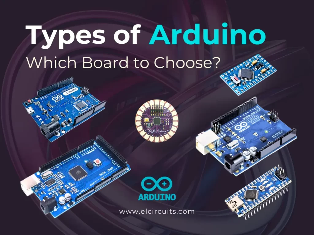
- Arduino Mega 2560 R3: Complete Pinout and Key Features
- What is Arduino?
- How to Install Arduino Software (IDE) on Windows – Step by Step!
Summary of Electrical Characteristics and Limitations
-
Microcontroller: The board is equipped with the
ATmega328Pchip, operating at a clock frequency of16 MHz. -
Operating Voltage: The board operates at a voltage of
5V, which is internally regulated from an external source (VIN pin) or from the USB connection. -
Power Supply (VIN): The
VINpin accepts an input voltage recommended between7Vand12V. The absolute range can reach 6-20V, but higher voltages may overheat the regulator. -
Current per I/O Pin: Each digital I/O pin can supply or
receive a maximum of
20mAof current. The absolute maximum value is 40mA, but exceeding 20mA can permanently damage the pin. -
Total Current I/O Pins: The sum of currents from all I/O
pins and the
5Vpin should not exceed200mA. -
USB-Serial Converter: Communication with the computer is
managed by an
ATmega16U2chip, which acts as a USB to serial converter, allowing programming and debugging via a virtual serial port. -
Memory: The
ATmega328Phas32KBof Flash memory (for code, with 0.5KB used by the bootloader),2KBof SRAM (for variables), and1KBof EEPROM (for non-volatile data storage). -
Analog Input Pins (ADC): It has
6analog input pins (A0-A5) with a resolution of10 bits(values from 0 to 1023).
Understanding the pinout and electrical characteristics of the Arduino UNO R3 is the first step to creating robust and functional electronic projects. This guide serves as a quick reference to avoid common mistakes, such as overloading a pin or using an inadequate power supply. Mastering these concepts, you will be ready to explore the entire universe of possibilities that the Arduino platform offers, from simple LED activations to complex automation and IoT systems.
🤔 Frequently Asked Questions (FAQ): About the Arduino UNO R3 Pinout
To ensure your project is a success, we’ve compiled some of the most common questions about the Arduino UNO R3 pinout. Check it out!
What is the difference between the VIN and 5V pins? 🔽
The VIN pin is a raw voltage input (recommended 7-12V) that powers the board’s voltage regulator, which in turn generates the stable 5V. The 5V pin is the already regulated output. You can power the Arduino through the 5V pin, but you must ensure that the source is exactly 5V and stable, as this bypasses the voltage regulator, which can be risky for the microcontroller.
Why do some digital pins have a tilde (~) next to the number? 🔽
The tilde (~) indicates that the pin supports PWM (Pulse Width Modulation or Pulse Width Modulation). These pins can simulate an analog output by varying the “width” of the voltage pulse at high frequency. It is widely used to control the brightness of LEDs or the speed of DC motors. On the Arduino UNO, the PWM pins are ~3, ~5, ~6, ~9, ~10, ~11.
Can I use the A0-A5 pins as digital pins? 🔽
Yes! The analog input pins (A0 to A5) can also function as digital pins. In the code, you can refer to them simply as A0, A1, etc., or using their equivalent digital pin numbers (A0 is 14, A1 is 15, and so on up to A5 which is 19).
How do the I2C and SPI communication pins work? 🔽
I2C uses two pins: SDA (data line) on pin A4 and SCL (clock line) on pin A5. It is a communication protocol with multiple slaves and master. SPI uses four pins: MOSI (D11), MISO (D12), SCK (D13) and SS (D10). It is faster than I2C, ideal for high-speed communication with devices like displays and SD cards.
What happens if I exceed the maximum current of an I/O pin? 🔽
Exceeding the maximum current of 20mA (recommended value) per pin can permanently damage the GPIO port of the ATmega328P microcontroller. This can make the pin unusable for input or output. To drive loads that require more current (like motors or relays), always use a driver circuit, such as a transistor or a relay module.
What is the AREF pin used for? 🔽
The AREF (Analog Reference) pin is used to provide an external and more precise reference voltage for the analog-to-digital converter (ADC) conversions. By default, the Arduino uses 5V as the reference, which means a reading of 1023 corresponds to 5V. If you connect a more stable and precise voltage (e.g., 3.3V) to the AREF pin, you can improve the accuracy of your analog readings, especially when working with sensors that operate in a lower voltage range.
✨ Our Gratitude and Next Steps
We sincerely hope this guide has been useful and enriching for your projects! Thank you for dedicating your time to this content.
Your Feedback is Invaluable:
Have any questions, suggestions, or corrections? Feel free to share them in the comments below! Your contribution helps us refine this content for the entire ElCircuits community.
If you found this guide helpful, spread the knowledge!
🔗 Share This GuideBest regards,
The ElCircuits Team ⚡