Português
 Español
Arduino Mega 2560 R3: Complete Pinout and Key Features

The Arduino Mega 2560 R3 is one of the most robust and popular development boards in the Arduino family, designed for projects that require a large number of input and output pins. Its extensive number of digital and analog ports makes it the ideal choice for complex applications such as 3D printers, robots, lighting controllers, and home automation systems.
In this complete guide, we will detail the pinout of the Arduino Mega 2560 R3. We will cover the functions of each pin, its electrical characteristics, limitations, and provide a quick reference table to help you maximize the potential of this board in your projects.
I/O (Input/Output) Pin Table
| Pin on Board | GPIO (Chip) | Main Functions | Critical Notes / Default State |
|---|---|---|---|
D0 / RX0
|
PD0 | UART0 (Receive) | Conflicts with USB serial communication. Default State: Input. |
D1 / TX0
|
PD1 | UART0 (Transmit) | Conflicts with USB serial communication. Default State: Input. |
D2 / RX1
|
PD2 | UART1 (Receive), External Interrupt 0 | Default State: Input. |
D3 / TX1
|
PD3 |
UART1 (Transmit), PWM, External Interrupt 1
|
Default State: Input. |
D4
|
PD4 | – | Default State: Input. |
D5 ~
|
PD5 |
PWM
|
Default State: Input. |
D6 ~
|
PD6 |
PWM
|
Default State: Input. |
D7
|
PD7 | – | Default State: Input. |
D8
|
PB0 | – | Default State: Input. |
D9 ~
|
PB1 |
PWM
|
Default State: Input. |
D10 ~ / SS
|
PB2 |
PWM, SPI (Slave Select)
|
Default State: Input. |
D11 ~ / MOSI
|
PB3 |
PWM, SPI (Master Out)
|
Default State: Input. |
D12 / MISO
|
PB4 |
SPI (Master In)
|
Default State: Input. |
D13 / SCK
|
PB5 |
SPI (Clock), LED L
|
Connected to onboard LED. Default State: Input. |
D14 / TX3
|
PJ1 | UART3 (Transmit) | Default State: Input. |
D15 / RX3
|
PJ0 | UART3 (Receive) | Default State: Input. |
D16 / TX2
|
PH1 | UART2 (Transmit) | Default State: Input. |
D17 / RX2
|
PH0 | UART2 (Receive) | Default State: Input. |
D18 / TX1
|
PD3 | UART1 (Transmit) | Default State: Input. |
D19 / RX1
|
PD2 | UART1 (Receive) | Default State: Input. |
D20 / SDA
|
PD1 |
I2C (Data)
|
Default State: Input. |
D21 / SCL
|
PD0 |
I2C (Clock)
|
Default State: Input. |
D22
|
PA0 | – | Default State: Input. |
D23
|
PA1 | – | Default State: Input. |
D24
|
PA2 | – | Default State: Input. |
D25
|
PA3 | – | Default State: Input. |
D26
|
PA4 | – | Default State: Input. |
D27
|
PA5 | – | Default State: Input. |
D28
|
PA6 | – | Default State: Input. |
D29
|
PA7 | – | Default State: Input. |
D30
|
PC7 | – | Default State: Input. |
D31
|
PC6 | – | Default State: Input. |
D32
|
PC5 | – | Default State: Input. |
D33
|
PC4 | – | Default State: Input. |
D34
|
PC3 | – | Default State: Input. |
D35
|
PC2 | – | Default State: Input. |
D36
|
PC1 | – | Default State: Input. |
D37
|
PC0 | – | Default State: Input. |
D38
|
PD7 | – | Default State: Input. |
D39
|
PG2 | – | Default State: Input. |
D40
|
PG1 | – | Default State: Input. |
D41
|
PG0 | – | Default State: Input. |
D42
|
PL7 | – | Default State: Input. |
D43
|
PL6 | – | Default State: Input. |
D44
|
PL5 | – | Default State: Input. |
D45
|
PL4 | – | Default State: Input. |
D46
|
PL3 | – | Default State: Input. |
D47
|
PL2 | – | Default State: Input. |
D48
|
PL1 | – | Default State: Input. |
D49
|
PL0 | – | Default State: Input. |
D50 / MISO
|
PB3 |
SPI (Master In)
|
Default State: Input. |
D51 / MOSI
|
PB2 |
SPI (Master Out)
|
Default State: Input. |
D52 / SCK
|
PB1 |
SPI (Clock)
|
Default State: Input. |
D53 / SS
|
PB0 |
SPI (Slave Select)
|
Default State: Input. |
A0
|
PF0 | Analog Input |
Can also be used as digital pin D54. Default State: Input.
|
A1
|
PF1 | Analog Input |
Can also be used as digital pin D55. Default State: Input.
|
A2
|
PF2 | Analog Input |
Can also be used as digital pin D56. Default State: Input.
|
A3
|
PF3 | Analog Input |
Can also be used as digital pin D57. Default State: Input.
|
A4
|
PF4 | Analog Input |
Can also be used as digital pin D58. Default State: Input.
|
A5
|
PF5 | Analog Input |
Can also be used as digital pin D59. Default State: Input.
|
A6
|
PF6 | Analog Input |
Can also be used as digital pin D60. Default State: Input.
|
A7
|
PF7 | Analog Input |
Can also be used as digital pin D61. Default State: Input.
|
A8
|
PK0 | Analog Input |
Can also be used as digital pin D62. Default State: Input.
|
A9
|
PK1 | Analog Input |
Can also be used as digital pin D63. Default State: Input.
|
A10
|
PK2 | Analog Input |
Can also be used as digital pin D64. Default State: Input.
|
A11
|
PK3 | Analog Input |
Can also be used as digital pin D65. Default State: Input.
|
A12
|
PK4 | Analog Input |
Can also be used as digital pin D66. Default State: Input.
|
A13
|
PK5 | Analog Input |
Can also be used as digital pin D67. Default State: Input.
|
A14
|
PK6 | Analog Input |
Can also be used as digital pin D68. Default State: Input.
|
A15
|
PK7 | Analog Input |
Can also be used as digital pin D69. Default State: Input.
|
Power and Control Pin Table
| Pin on Board | Name | Function | Technical Description |
|---|---|---|---|
VIN
|
Input Voltage | External Power |
Pin to power the board with an external source (recommended
7-12V). The voltage is regulated to 5V by the
onboard regulator.
|
5V
|
5 Volts | Regulated Power |
Provides regulated 5V from the onboard regulator or from
the USB connection. Used to power external components that operate at
5V.
|
3.3V
|
3.3 Volts | Regulated Power |
Provides regulated 3.3V from an onboard buck converter.
Maximum current of 50mA.
|
GND
|
Ground | Ground | Ground reference pins (0V). There are several GND pins on the board. |
AREF
|
Analog Reference | Analog Reference |
Pin to provide an external reference voltage (between
0V and 5V) for the analog inputs, improving
the accuracy of ADC conversions.
|
RESET
|
Reset | Reset Microcontroller |
Setting this pin to low (LOW) resets the ATmega2560
microcontroller. Generally used with an external reset button.
|
Schematic Diagram
The schematic diagram of the Arduino Mega 2560 R3 provides a detailed view of the electrical connections between the board’s components. It is essential for understanding how power is distributed, how peripherals connect to the microcontroller, and how USB communication is implemented. Analyzing the schematic is fundamental for advanced debugging and for projects that modify or interact with the board’s low-level circuits.

🔗 Related Content
If you liked this project, you might also be interested in these other articles:
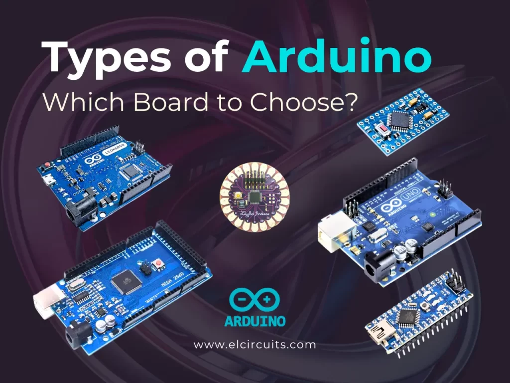
- Arduino UNO R3: Pinout and Key Features
- What is Arduino?
- How to Install Arduino Software (IDE) on Windows – Step by Step!
Summary of Electrical Characteristics and Limitations
- Main Microcontroller: ATmega2560, an 8-bit chip with AVR architecture, offering 256 KB of Flash memory, 8 KB of SRAM, and 4 KB of EEPROM.
-
Operating Voltage: The board operates at
5V, however, the ATmega2560 microcontroller can operate with a voltage range of2.7Vto5.5V. -
Power (VIN): The recommended input voltage for the
VINpin is7Vto12V. The absolute maximum range is6Vto20V. Voltages above12Vmay overheat the voltage regulator. -
Current per I/O Pin: Each digital I/O pin can supply or
receive a maximum of
20mAof current. The total current for all I/O pins should not exceed200mA. -
I/O and PWM Pins: It has 54 digital I/O pins, of which 15
can be used as
PWM(Pulse Width Modulation) outputs to control LED brightness, motor speed, etc. - Analog Inputs: It has 16 analog inputs with 10-bit resolution (values from 0 to 1023), allowing reading of sensors and other analog devices.
- USB-Serial Converter: It uses a dedicated ATmega16U2 chip for USB communication, providing a stable and reliable virtual serial connection with the computer, without the need for FTDI drivers.
- Communication: Includes 4 UART (serial) ports, 1 I2C port, and 1 SPI port, allowing communication with a wide range of peripherals and other microcontrollers.
Understanding the pinout of the Arduino Mega 2560 R3 is the first step to unlocking its full potential. This guide serves as a quick reference to help you connect your components correctly, avoid common mistakes, and make the most of the features of this powerful board. Whether building a complex robot or an automation system, detailed knowledge of each pin is the foundation for a successful project.
🤔 Frequently Asked Questions (FAQ)
To ensure your project is a success, we’ve compiled some of the most common questions about the Arduino Mega 2560 R3 pinout. Check it out!
1. What is the difference between VIN and 5V pins? 🔽
The VIN pin is used to power the board with an external
unregulated voltage source (recommended between 7V and
12V). This voltage passes through an onboard regulator that
converts it to 5V. The 5V pin, in turn,
provides this already regulated voltage (whether from VIN or the USB
port) and can be used to power external components that operate at
5V. Never connect a voltage higher than
5V directly to the 5V pin, as this can damage
the board.
2. How many PWM pins does the Arduino Mega 2560 have and which are they? 🔽
The Arduino Mega 2560 has 15 pins that support PWM (Pulse
Width Modulation) output. They are: ~2, ~3,
~5, ~6, ~7, ~8,
~9, ~10, ~11, ~12,
~13, ~44, ~45, ~46.
The ~ symbol next to the pin number on the board indicates
its PWM capability.
3. Can I use the analog pins (A0-A15) as digital pins? 🔽
Yes, you can. The analog input pins A0 to
A15 can also function as digital pins. In Arduino code, you
can refer to them using their analog pin names (e.g.,
pinMode(A0, OUTPUT)) or their equivalent digital pin
numbers (A0 is D54, A1 is
D55, and so on up to A15 which is
D69).
4. What is the AREF pin and when should I use it? 🔽
The AREF (Analog Reference) pin allows you to provide an
external reference voltage for analog-to-digital (ADC) conversions. By
default, Arduino uses 5V as reference, which means a
reading of 1023 corresponds to 5V. If you’re working with
sensors that operate in a smaller voltage range (for example,
0V to 3.3V), you can apply
3.3V to the AREF pin to get higher resolution
and more accurate readings in that range. Be careful not to apply a
voltage higher than 5V to the AREF pin.
5. Why are pins D0 and D1 not recommended for general use? 🔽
Pins D0 (RX) and D1 (TX) are used for serial
communication (UART0) with the computer through the USB port. If you use
these pins for other purposes, you may interfere with the ability to
upload new sketches or serial communication with the Serial Monitor.
It’s better to avoid using them unless you don’t need USB communication
or are using the other UART ports (Serial1,
Serial2, Serial3).
6. What is the function of the ATmega16U2 chip on the board? 🔽
The ATmega16U2 chip functions as a USB-Serial converter.
It manages communication between your computer’s USB port and the main
UART port (D0/D1) of the main
ATmega2560 microcontroller. This allows the board to appear
as a virtual COM port device on the computer, facilitating programming
and debugging through the Serial Monitor, without the need for external
FTDI chips or proprietary drivers.
✨ Our Gratitude and Next Steps
We sincerely hope this guide has been useful and enriching for your projects! Thank you for dedicating your time to this content.
Your Feedback is Invaluable:
Have any questions, suggestions, or corrections? Feel free to share them in the comments below! Your contribution helps us refine this content for the entire ElCircuits community.
If you found this guide helpful, spread the knowledge!
🔗 Share This GuideBest regards,
The ElCircuits Team ⚡