Português
 Español
5-Band Active Graphic Equalizer (LF353 IC) + PCB Guide

Hello, electronics and high-fidelity audio enthusiast!
If you loved our 3-band equalizer project, get ready for an impressive evolution. Today, we present the definitive project for sound control: a 5-band active graphic equalizer, using the same and versatile LF353 IC. This circuit elevates your control to a new level, allowing you to finely adjust the frequencies bass, low-mid, mid, high-mid and treble, offering unprecedented power over the sound of your system.
The heart of this project continues to be the LF353, a high-performance JFET operational amplifier, celebrated for its exceptional bandwidth, extremely low noise, and ability to preserve the purity of the audio signal. With the addition of two more frequency bands, you can now correct acoustic deficiencies in the environment, enhance specific details of instruments, or simply shape the sound exactly as you've always dreamed.
💡 Professor's Tip: The great advantage of operational amplifiers with JFET input, like the LF353, is their extremely high input impedance (10¹²Ω). This means that the equalizer circuit practically does not "load" the signal source (your audio device, instrument, etc.), ensuring that the audio reaches the circuit with maximum integrity and without quality loss. Think of it as a perfect electronic "ear"!
⚙️ Technical Characteristics of the LF353 IC
The reasons for choosing the LF353 remain the same, being the backbone for high-quality audio:
- Internally Adjusted Offset Voltage: 10 mV
- Low Input Bias Current: 50pA
- Low Input Noise Voltage: 25 nV/√Hz
- Low Input Noise Current: 0.01 pA/√Hz
- Wide Gain Bandwidth: 4 MHz
- High Slew Rate: 13V/μs
- Low Supply Current: 3.6 mA
- High Input Impedance: 10¹²Ω
- Low Total Harmonic Distortion: ≤0.02%
- Low 1/f Noise: 50 Hz
- Fast Settling Time (0.01%): 2 μs
🎓 Deepening Knowledge: The slew rate of 13V/μs is crucial for high-fidelity audio. It determines how quickly the amplifier can respond to abrupt changes in the signal, such as the attack of a conga or the "pluck" of a guitar string. A high slew rate ensures that these transients are reproduced with clarity and precision, without distortion.
🛠️ How the 5-Band Equalizer Circuit Works
Our 5-band equalizer expands the previous concept, using multiple LF353 ICs to create independent active filters for each frequency range. The "magic" continues in the capacitors and resistors, which are now calculated to define five precise cutoff points, covering the entire audible spectrum in a more granular way.
This project is a 5-band graphic equalizer with control, with strategically chosen cutoff frequencies at: 100Hz, 330Hz, 1kHz, 3.3kHz and 10kHz. These points offer a much more detailed control:
- 100Hz: Controls the sub-bass and the "punch" of kick drums and basses.
- 330Hz: Responsible for the "body" of sounds, preventing bass from sounding muffled or mids from sounding "boxy".
- 1kHz: The central range of human speech intelligibility and many instruments.
- 3.3kHz: Defines the presence and clarity of vocals, guitars and cymbals.
- 10kHz: Adds brightness, "air" and definition to high frequencies, such as string harmonics and cymbal "sizzle".

For this 5-band project, you will need two LF353 ICs (or equivalents like the TL072, which also has two op-amps per IC), totaling 4 amplifiers. Each band will use one amplifier, and the fourth will be used as a buffer output stage, ensuring a low output impedance and protection for the next circuit. Substitutes like LM1558, RC4558 or LM358 can be used, but the LF353 remains the premium choice for audio.
The recommended supply voltage remains between ±11V and ±15V, with maximum support of ±18V. The current consumption will be slightly higher due to the second IC, but still remains quite efficient.
🔧 Assembly Tip: The cascade configuration (one filter after another) is fundamental. The audio signal passes through each filter stage, and each potentiometer adjusts the gain (attenuation or boost) of its respective frequency band. The final stage (buffer) ensures that the equalized signal is delivered to the output with strength and clarity, without being affected by the load of the next equipment (amplifier, mixer, etc.).
🔌 Circuit Schematic Diagram
In Figure 3 below, we present the conceptual schematic of the 5-band equalizer circuit. Remember to use the files from your own project for assembly. The download files are available in the section at the end of this article.

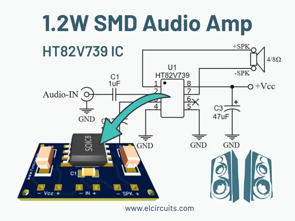
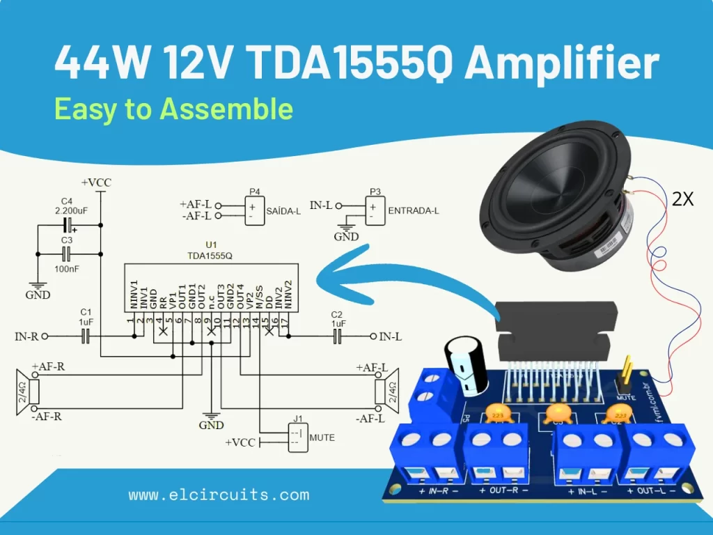
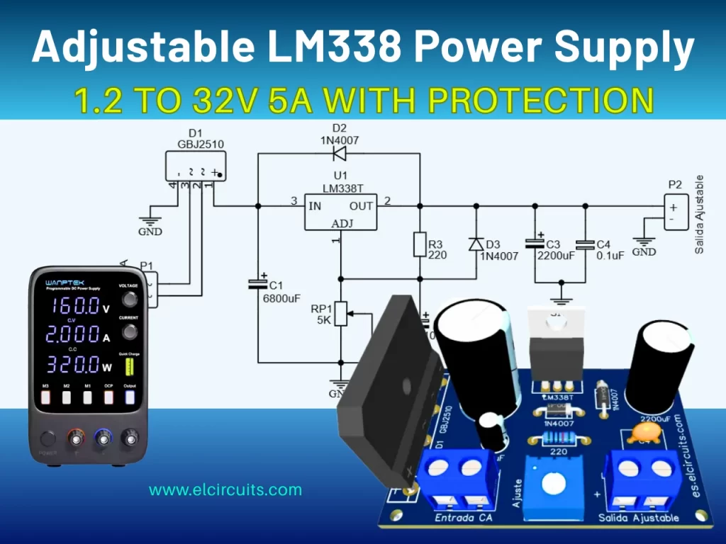
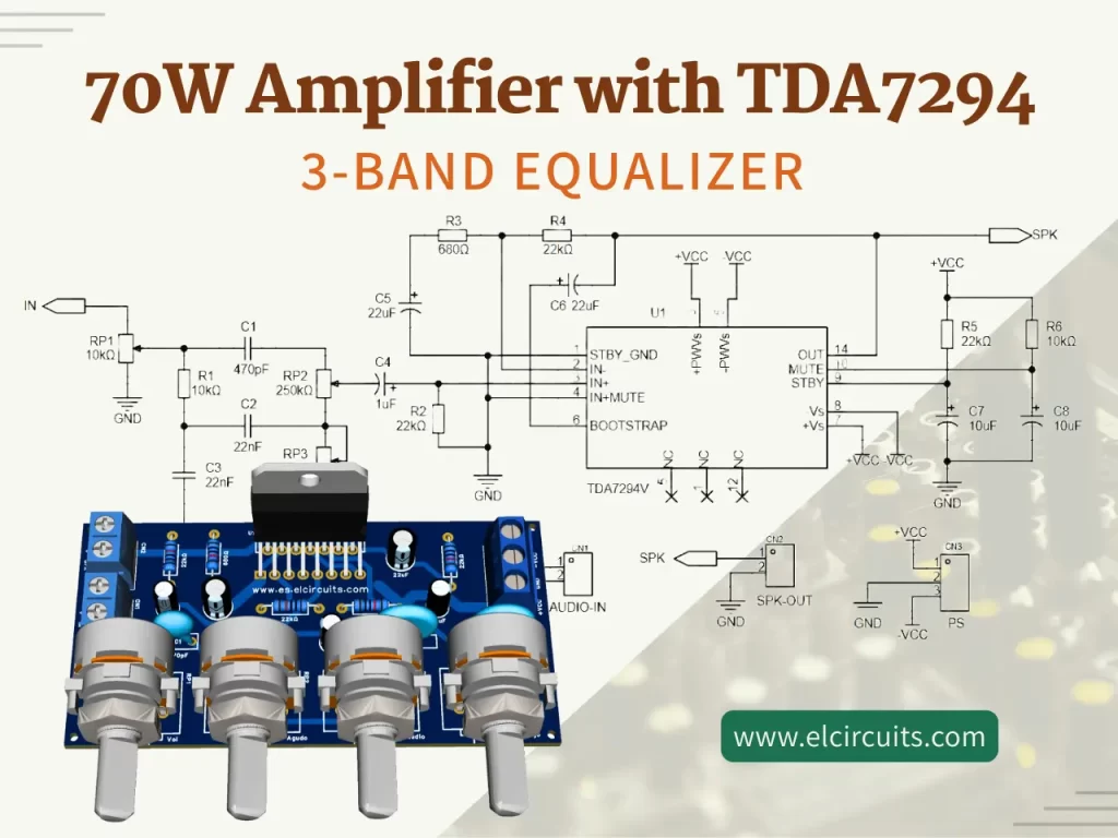
💡 Fresh Ideas for Your Next Project
Did you enjoy this project? Then you'll love exploring other circuits we've prepared. Each one with its unique features and ideal applications!
🛠️ Component List
To build your 5-band equalizer, you will need the following components:
- U1, U2, U3 .... LF353 Integrated circuit
- R1 .................. 47K resistor (yellow, purple, orange, gold)
- R2 to R11 ...... 10K resistor (brown, black, orange, gold)
- R12 ................ 100K resistor (brown, black, yellow, gold)
- C1 ................... 680nF polyester capacitor
- C2, C3 ............ 150nF polyester capacitor
- C4 ................... 33nF polyester capacitor
- C5 ................... 39nF polyester capacitor
- C6, C7 ............ 8.2nF polyester capacitor
- C8, C9 ............ 2.2nF polyester capacitor
- C10 ................. 470pF polyester capacitor
- C11 ................. 4.7uF electrolytic capacitor
- VR1 to VR5 ... 47K Potentiometer
- P1 ................... Screw Terminal Type 5mm 3-Pin Connector
- P2, P3 ............. Screw Terminal Type 5mm 2-Pin Connector
- Others ............. PCB, tin, wires, etc.
🔍 Expert Tip: For professional results, invest in high-quality potentiometers with logarithmic taper (type "A"). They offer a more natural response to the human ear for volume and tone applications. Use metal film resistors (1% tolerance) and polyester or polypropylene capacitors to ensure precise frequency response and lower distortion.
🖨️ Printed Circuit Board (PCB)
To facilitate your assembly, the Printed Circuit Board (PCB) files for the 5-band equalizer are available. The layout was designed to accommodate the additional components, minimizing noise and interference between the audio traces.

The files are available in GERBER, PDF and PNG formats, ready for manufacturing or home assembly. The PCB layout follows best practices for audio circuits, with signal and power traces properly separated and star grounding to avoid ground loops.
📥 Direct Download Link
To download the necessary files to build the electronic circuit, simply click on the direct link provided below:
🔧 Assembly and Testing Guide
The assembly process is similar to the 3-band project, but with some additional steps:
- Insert the smaller components: Start by soldering the resistors and diodes (if any). Check the orientation of polarized components.
- Soldering the capacitors: Install the polyester and electrolytic capacitors, paying close attention to polarity.
- Install sockets for the ICs: It is highly recommended to use sockets for the two LF353s. This facilitates replacement and protects the ICs during soldering.
- Install the potentiometers: Position the 5 potentiometers as indicated on the front panel layout.
- Power and signal connectors: Install the screw terminals for signal input/output and power supply.
- Insert the LF353 ICs: After the soldering cools, insert the ICs into the sockets, checking the correct orientation (usually a notch or dot indicates pin 1).
- Visual inspection: Check all connections, possible short circuits or cold solder joints.
- Initial test: Connect a symmetrical power supply (±12V recommended) without input signal and check if there is no abnormal heating in the ICs.
- Test with signal: Apply an audio signal and test the operation of each of the 5 bands individually.
⚠️ Safety Alert: Always turn off the power before handling the circuit. Use a symmetrical power supply with current limiting to protect the ICs during initial tests. When soldering, work in a well-ventilated environment and use appropriate protective equipment.
🎵 Applications and Possibilities
Your new 5-band active equalizer opens a universe of possibilities for audio control:
🎸 Musical Instruments
- Perfect for luthiers and musicians who want to create a custom tone circuit for guitars, basses and keyboards, with much finer control over the timbre.
🔊 Home Sound Systems
- Ideal for correcting specific acoustic deficiencies in your living room, adapting the frequency response of your speakers with surgical precision.
🎧 Home Studios and Music Production
- A powerful tool for adjusting sound during recordings or in the final mix. Use to give more "presence" to a vocal, cut the "mud" from a bass or add "brightness" to a cymbal track.
📡 PA Systems and Sound Reinforcement
- Can be integrated into sound systems for small events or churches, allowing fine adjustments to compensate for the acoustic characteristics of the environment.
💡 Professor's Tip: To experiment with the effects of the equalizer, try these initial settings: for a "V-shape" sound (boosted bass and treble, popular in some musical styles), increase the 100Hz and 10kHz controls and slightly attenuate the 1kHz one. For a "warmer" and vocal-friendly sound, boost the 330Hz and 1kHz bands. Remember: the ear is the final judge!
🤔 Frequently Asked Questions (FAQ)
To ensure your project is a success, we've compiled some of the most common questions on this topic. Check them out!
How many LF353 ICs are needed for the 5-band equalizer? 🔽
For the 5-band equalizer, you will need three LF353 ICs. Each LF353 contains two operational amplifiers (op-amps). Five bands require five op-amps, and one more is needed for the buffer output stage, totaling six op-amps. Therefore, three LF353 ICs (3x2=6 op-amps) are sufficient.
What is the function of the two new frequency bands (330Hz and 3.3kHz)? 🔽
Excellent question! The 330Hz (low-mid) band is crucial for giving "body" and "weight" to sounds, controlling the sound of guitar cabinets, the "presence" of a vocal or preventing bass from sounding "loose". The 3.3kHz (high-mid) band is where the "intelligibility" and "presence" of many instruments reside. Adjusting this band can make a vocal stand out in the mix or give more "attack" to drums. These two bands offer control that the 3-band equalizer simply couldn't reach.
Is it possible to convert this mono equalizer to stereo? 🔽
Yes, it's totally possible, but it will require double the components. You'll need to build an identical circuit for the right channel and another for the left channel. This means using double the ICs, resistors, capacitors and, crucially, dual potentiometers (two potentiometers on a single shaft, one for each channel) so you can adjust both channels simultaneously with a single knob. The PCB layout will also need to be adapted to accommodate all the additional components.
What is the best power supply voltage for this equalizer? 🔽
The recommended supply voltage remains between ±11V and ±15V. A ±12V symmetrical supply is ideal for most applications, offering a good balance between performance (headroom) and power consumption. The IC supports up to ±18V maximum, but higher voltages may generate more heat without necessarily improving audio quality in a perceptible way.
🎓 Conclusion and Next Steps
Congratulations! With this project, you now have a high-quality 5-band active equalizer, an extremely versatile and powerful tool for any audio enthusiast. This project not only offers unprecedented control over sound, but also represents excellent learning about audio circuit design, active filters, and signal processing.
✨ Our Gratitude and Next Steps
We sincerely hope this guide has been useful and enriching for your projects! Thank you for dedicating your time to this content.
Your Feedback is Invaluable:
Have any questions, suggestions, or corrections? Feel free to share them in the comments below! Your contribution helps us refine this content for the entire ElCircuits community.
If you found this guide helpful, share the knowledge!
🔗 Share This GuideBest regards,
The ElCircuits Team ⚡