Showing posts with label power supply. Show all posts

Friday, April 14, 2023

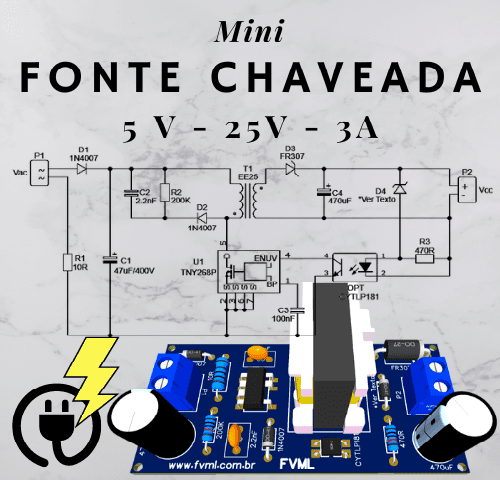
Mini Switching Power Supply 5V - 25V, 3A with TNY268 and PCB

Mini Switching Power Supply 5V - 25V, 3A with TNY268 and PCB

Para Versão em Portugues, clique aqui!

Compact 3A Mini Switching Power Supply: Build Your Own 5V-25V Solution with TNY268 and PCB

In this article, we will be discussing a mini switched power supply that provides 5V to 25Vdc output. This power supply is perfect for various electronic devices that require a stable and reliable power supply.

This is a power supply based on the TNY268 Integrated Circuit, which is part of a series of TinySwitch-II circuits: TNY263, TNY264, TNY265, TNY266, TNY267 and TNY268.

For a Flyback-type switched power supply like the one proposed, this IC is ideal, it integrates in its encapsulation the components necessary for it to work:

  • PWM Control, Power Mosfets
  • Overcurrent Protection
  • Over-Temperature Protection
  • Self-Feeding System

It does not need auxiliary windings, which makes it a complete IC, with DIP8 encapsulation, with a PWM working frequency of 132kHz and a voltage of up to 700V.

We will dive into the technical specifications, design, and features of this power supply and how it compares to other similar products in the market.

Technical Specifications

The mini switched power supply has an input voltage range of 80V to 260V AC, which makes it suitable for use in different parts of the world.

It provides an output voltage that can be regulated between 5V to 25V, with a current of up to 3A, depending on the configuration that we choose.

The power supply also has short-circuit protection and overvoltage protection, ensuring the safety of the connected devices.

Design

The mini switched power supply has a compact design, with dimensions of 55mm x 26mm x 21mm. The power supply is enclosed in a plastic case that protects the circuitry from dust and other environmental factors.

The power supply has a standard WJ2EDGVC-5.08-2P connector, making it easy to connect different electronic devices.

Caution!

"This circuit works directly connected to the electrical network, this is extremely dangerous, any carelessness, or wrong connections, design error, or any other occasion, can lead to irreversible damage.

We are not responsible for any type of occurrence. If you don't have enough experience, don't build this circuit, and if you build it, when testing it, be sure to have the proper protections and be accompanied by someone else."

Features

One of the standout features of this mini switched power supply is its efficiency. It has a high efficiency rating of up to 85%, which means that it wastes less energy as heat compared to other similar products.

This feature is especially important for electronic devices that are battery-powered, as it helps to extend their battery life.

Another feature of this power supply is its low ripple and noise. The power supply has a ripple voltage of less than 50mV, which ensures that the connected devices receive a stable and noise-free power supply. 

This is especially important for audio devices, where any noise in the power supply can cause unwanted noise in the audio output.

TNY268 - Pinout and Description

The TNY268 is packaged in a DIP-8B structure for perforated pinouts and an SMD-8B package for SMD.

The package is similar to the well-known IC LM555, with the exception of pin 6 hidden in the TNY268, as we can see in the pinout of Figure 2, below.

Fig. 2 - Pinout - Pinout TNY268

We leave below the description of each pin of the TNY268 Integrated Circuit to facilitate our understanding.

  • DRAIN (D): Power MOSFET drain connection. Provides internal operating current for start-up and steady-state operation.

  • BYPASS (BP): Connection point for an external 0.1 µF bypass capacitor for the internally generated 5.8 V supply.

  • ENABLE/UNDERVOLTAGE (EN/UV): This pin has two functions: input enable and line undervoltage detection. During normal operation, power MOSFET switching is controlled by this pin. MOSFET switching is terminated when a current greater than 240 μA is drawn from this pin.

    This pin also detects line undervoltage conditions through an external resistor connected to the DC line voltage. If there is no external resistor connected to this pin, TinySwitch-II detects its absence and disables the line undervoltage function.

  • SOURCE (S): Common control circuit, connected internally to the output MOSFET source.

  • SOURCE (HV RTN): MOSFET source connection output for high voltage feedback.

The Switched Power Supply Circuit

The Mini Switched Power Supply Circuit with TNY268 for 5V - 24V, 3A output is a simple yet powerful design, as shown in Figure 3 below.

However, due to the involvement of electricity, it requires careful handling and at least intermediate knowledge of electronics to assemble the circuit.

Fig. 3 - Schematic Diagram Mini Switching Power Supply 5V - 25V, 3A with TNY268

The schematic diagram of the Mini Switched Power Supply Circuit is well laid out and easy to understand. It includes a TNY268 controller that regulates the output voltage and current of the power supply.

The circuit has a few essential components such as capacitors, resistors, diodes, and an inductor, which work together to provide stable and efficient power.

Regulate The Output Voltage

The output voltage is adjusted through two parameters in the circuit:

  1. The D4 diode, which is a 1W Power Zener diode.
  2.  The secondary winding of the transformer.

The Zener Diode

The zener diode D4, is the diode that will adjust the output voltage, we must configure it as follows,
when the desired voltage is Xv, the zener diode must have a voltage Xv - 1.

The diode should be 1V lower than the nominal voltage of the power supply, this lower voltage is due to the photocoupler being connected in series with the zener diode, and since it is an “LED” diode, we have the voltage drop on it.

For example:

To obtain a voltage of 5V at the power supply output:
The zener diode D4 = 4V. We use a commercial 4.3V, 1N4731 zener diode.

To obtain a voltage of 9V at the power supply output:
The zener diode D4 = 8V. We use a commercial 8.2V, 1N4738 zener diode.

To obtain a voltage of 12V at the power supply output:
The zener diode D4 = 11V. We use a commercial 11V, 1N4741 zener diode.

To obtain a voltage of 25V at the power supply output:
The zener diode D4 = 24V. We use a commercial 24V, 1N4749 zener diode.

The Transformer

The transformer used in this circuit was a high frequency transformer, often found in PC power supplies, as illustrated in Figure 4 below, a model EE-25 Ferrite transformer.

Fig. 4 EE-25 Ferrite Transformer

Primary coil winding

The primary will be wound to support a voltage between 85V and 260V, and this will be done by winding 140 turns of 33AWG enamelled wire, or 0.18 mm diameter wire.

Right after winding the primary, place appropriate insulation tape, with electrical and thermal insulation, to insulate the primary from the secondary.

Secondary coil winding

The secondary will be wound according to the desired output voltage, and this will be done in such a way that, for each desired 1V, 1.4 turns of 17AWG enameled wire or 1.15 mm wire are wound.

The calculation for an output voltage of 5V can be achieved using the formula below:

Formula: N = V * F
  • N = Number of Turns
  • V = Desired Voltage
  • C = Constant = 1.4
  • V = 5V
  • C = 1.4
  • N = ?
  • N = 5 * 1.4
  • N = 7 laps
For 5V on the output, we have 7 turns to wind in the secondary.

The calculation for an output voltage of 9V:

  • V = 9V
  • F = 1.4
  • N = ?

  • N = 9 * 1.4
  • N = 12.6 = ~13 Rounds
For 9V on the output, we have 13 turns to wind in the secondary.

The calculation for an output voltage of 12V:

  • V = 12V
  • F = 1.4
  • N = ?

  • N = 12 * 1.4
  • N = 16.8 = ~17 Rounds
For 12V output, we have 17 turns to wind in the secondary.

The calculation for an output voltage of 24V:

  • V = 25V
  • F = 1.4
  • N = ?

  • N = 25 * 1.4
  • N = 35 Turns

For 24V output, we have 37 turns to wind in the secondary.

The good thing is that with the formula, we can calculate any voltage we want to get at the output of our switching power supply.

Components list

Semiconductor

  • U1 ......... Integrated Circuit TNY268P
  • OPT....... TLP181 Opto-Coupler
  • D1, D2 ... Diode 1N4007
  • D3 ......... Fast Diode FR307
  • D4 ......... Zener Diode *See Text

Resistor

  • R1 .... Resistor 10Ω / 1W (brown, black, black, gold)
  • R2 .... Resistor 200KΩ / 1/4W (red, black, yellow, gold)
  • R3 .... Resistor 470Ω / 1/4W (yellow, violet, brown, gold)

Capacitors

  • C1 ....... Electrolytic Capacitor 47uF/400V
  • C2 ....... Polyester Capacitor 2.2nF
  • C3 ....... Polyester Capacitor 100nF
  • C4 ....... Electrolytic Capacitor 470uF/35V

Several

  • T1 ......... EE-25 Ferrite Transformer
  • P1, P2 ... Connector WJ2EDGVC-5.08-2P
  • Others... PCI, Wires, Solders, Etc.

Printed Circuit Board - Download

In Figure 5 below, we are making the PCI available in GERBER, PDF and JPEG files, for those who want to create a more optimized assembly, either at home, or if you prefer, at a company that prints the board.

PCB-Mini Switching Power Supply 5V - 25V, 3A with TNY268

You can download the files for free from a direct link in the Download option below.

Conclusion

In conclusion, the mini switched power supply that provides a programable 5V to 25Vdc output is an excellent choice for various electronic devices. Its compact design, high efficiency, and low ripple and noise make it stand out compared to other similar products in the market.

Its safety features, such as short-circuit protection and overvoltage protection, ensure that connected devices are protected from damage. If you are looking for a reliable and efficient power supply for your electronic devices, then this mini switched power supply is a great choice.

You can see the official post by clicking here! fvml.com.br

I hope you enjoyed it!!!

If you have any questions, suggestions or corrections, please leave them in the comments and we will answer them soon.

Subscribe to our blog!!! Click here - elcircuits.com!!!

My Best Regards!!!

Monday, January 30, 2023

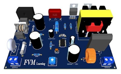
Switched Power Supply SMPS 13.8V 10A using IR2153 IC and IRF840, with PCB

13.8V-SMPS-Power-Supply-Using-IR2153-IC-and-IRF840-Mosfet

Para Versão em Portugues, clique aqui!

Switched Power Supply SMPS 13.8V 10A using IR2153 IC and IRF840, with PCB

This circuit is a straightforward design for an SMPS power supply, utilizing the IR2153 IC. This chip, which has only 8 pins, functions as a PWM controller, enabling the creation of a high-performing and cost-effective unregulated switching power supply for basic projects.

The output voltage of this power supply is set at 13.8V and can be adjusted via the trimpot RV1. It also provides a steady current of 10A at its output.

The Circuit

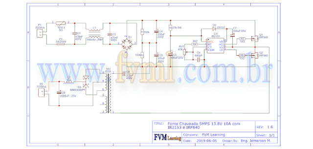
The circuit basically consists of 8 main steps:

  1. Protection Circuit: It comprises a 5A/250V fuse, which operates if there is a current greater than the fuse's breaking current.
    At the same time we also have an NTC (Negative Temperature Coefficient), it is a surge current limiter, this same topology can be found in most SMPS power supplies, such as notebook power supplies, PC power supplies, computer AT / ATX power supplies, etc.

  2. Transient Filter: This step consists of an initial capacitive filter that inhibits high frequencies from returning to the network, or vice versa, and soon after, the EMI filter coil, which serves to attenuate high frequency noise.

  3. Primary Rectification: Made up of the D1 rectifier bridge.

  4. Primary Filter: Composed of capacitors C4 and C5.

  5. Switching: Composed of a PWM generator, and the IRF840 power MOSFETS transistors.

  6. Transformer: The transformer is a high-frequency Chopper Trafo, and it performs the isolation and high-frequency transformation of the signal generated by the PWM set and switching transistors.

  7. Fast Rectification: Formed by diode D3, this is a fast and double diode, since the oscillated frequency in the circuit is quite high.

  8. Output filter: Composed of inductor L2 and capacitor C9.

Caution

This circuit works directly connected to the electrical network, this is extremely dangerous, any carelessness, or wrong connections, design error, or any other occasion, can lead to irreversible damage.

We are not responsible for any type of occurrence. If you don't have enough experience, don't build this circuit, and if you build it, when testing it, be sure to have the proper protections and be accompanied by someone else.

The PWM Circuit

The power supply for the IR2153 IC comes through a 27K 5W power-limiting resistor together with the C5 capacitor. In the internal package of this IC, there is already a 15.6V Zener diode, which stabilizes this voltage, but the current is low.

So, be careful not to put the resistor R3 with a smaller resistance, as it would increase the current at the input of the IC, and the Zener could break and consequently burn the IC.

An improved solution would be to put a 15V Zener diode to ensure voltage stabilization and IC protection, which you can be doing if you wish.

If you are using the IR2153D, there is no need to use the D2 diode which is the FR107 or BA159, as this IC already has this diode internally, if it is the IR2153without the letter D”, leave it as it is in the schematic, “ with diode D2”.

The complete schematic diagram is displayed just below in Figure 2, both the diagram and the materials are available for download at the link below.

Figure-2-Schematic-Diagram-SMPS-13.8V-10A-power-supply

The Transformer

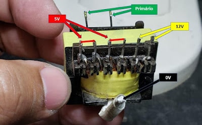
The TR1 transformer was taken from a scrap ATX power supply, the model is the IE-35A, but you can be using practically any model of ATX power supply Trafo.

There is no need to rewind the transformer, just pay attention to the Pinout that we will use for the Trafo, as shown in Figure 3 below.

Fig.3-ATX-power-supply-Trafo-wire-connection-diagram

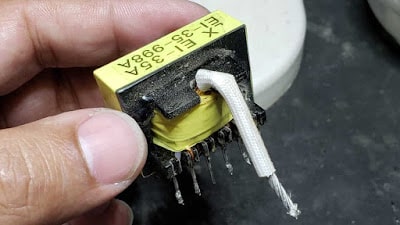
The Trafo model used was the EI-35A, but we can also use any other AT or ATX power supply that has the same standards, such as models EI-33, ER35, TM3341101QC, ERL35, EI28, etc., as shown in Figure 4 below.

Fig.4-ATX-power -supply-transformer-model-EI-35A

The L1 inductor is the same used in the ATX power supply, we removed it and didn't make any changes, and the L2 inductor, from the output EMI filter.

You can also use the AT/ATX power supply scrap, but if you want to wind your own filter, you can wind it on a Ferrite Toroidal core.

The winding must be carried out using a Toroidal core winding, with the coil using 0.6 mm super-enamelled copper wire with 25 turns.

Component List

  • Semiconductors
  • CI1 ......... Integrated Circuit IR2153D, or IR2153 (See Text)
  • Q1, Q2 ... IRF840 MOSFET transistors
  • D1 .......... KBU606 Diode Bridge (or Equivalent)
  • D2 .......... FR107 or BA159 Fast Diode (or Equivalent)
  • D3 .......... MBR3045PT Diodes Fast  (or Equivalent)

  • Resistors
  • R1, R2 .... 150KΩ resistor - (brown, green, yellow, gold)
  • R3 .......... 27KΩ 5W resistor – (red, violet, orange, gold)
  • R4 ...........8K2Ω resistor – (gray, red, red, gold)
  • R5, R6 ... 10Ω resistor – (brown, black, black, gold)
  • RV1 ....... 47kΩ trimpot 
  • NTC1..... 5Ω thermistor

  • Capacitors
  • C1, C2 ... 470nF - 400V Polyester Capacitor 
  • C3, C4 ... 330uF - 200V Electrolytic capacitor 
  • C5, C7 ... 100uF - 25V Electrolytic capacitor 
  • C6 .......... 680pF Polyester Capacitor 
  • C8 .......... 2.2uF - 400V Polyester Capacitor 
  • C9 .......... 2200uF - 25V Electrolytic capacitor 

  • Miscellaneous
  • L1, L2 .... Inductor *see text
  • TR1 ....... Transformer *see text
  • F1 .......... 5A Solderable fuse
  • Other...... Wire, Solder, Plate, Etc.

Printed Circuit Board

We provide the PCB - Printed Circuit Board, in GERBER, PDF and PNG files. These files are available for free download, on the MEGA server, in a direct link, without any bypass. 

All to make it easier for you to do a more optimized assembly, either at home, or with a company that prints the board. You can download the files in the Download option below.

Files to download, Direct Link:

Click on the link beside: GERBER, PDF and PNG files

You can see the official post by clicking here! fvml.com.br

I hope you enjoyed it!!!

If you have any questions, suggestions or corrections, please leave them in the comments and we will answer them soon.

Subscribe to our blog!!! Click here - elcircuits.com!!!

My Best Regards!!!

Wednesday, June 22, 2022

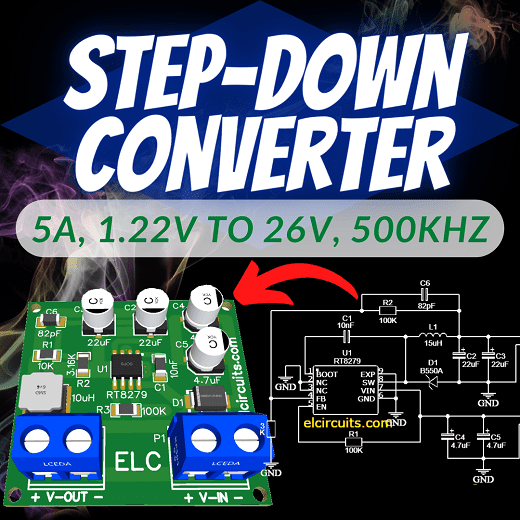
5A, 1.22V to 26V, 500kHz Step-Down Converter Using RT8289 IC with PCB

Fig. 1 - 5A, 1.22V to 26V, 500kHz Step-Down Converter Using RT8289 IC with PCB

Powerful 5A Step-Down Converter: Build a Versatile 1.22V to 26V Solution at 500kHz with RT8289 IC and PCB

This is a DC-DC 5A, 1.22V to 26V, 500kHz Step-Down Converter Using RT8289 IC, it works with a Step-Down conversion system.

This powerful chip manages to work with very few external components and provides a preset voltage between 1.22V to 26V, with 5 Amps of output current.

General  IC Description

The RT8289 is a step-down regulator with an internal Power MOSFET. It achieves 5A of continuous output current over a wide input supply range with excellent load and line regulation.

Current mode operation provides fast transient response and eases loop stabilization. The RT8289 provides protections such as cycle-by-cycle current limiting and thermal shutdown.

In shutdown mode, the regulator draws 25A of supply current. The  RT8289  requires  a  minimum  number  of  external components, to provide a compact solution. The  RT8289  is  available  in  a  SOP-8  (Exposed  Pad) package.

Features

  • High Output Current up to 5A
  • Internal Soft-Start
  • 100mΩ Internal Power MOSFET Switch 
  • Internal  Compensation  Minimizes  External  Parts Count
  • High Efficiency up to 90%
  • 25μA Shutdown Current
  • Fixed 500kHz Frequency
  • Thermal Shutdown Protection
  • Cycle-by-Cycle Over Current Protection
  • Wide 5.5V to 32V Operating Input Range
  • Adjustable Output  Voltage from 1.222V to 26V
  • Available in an SOP-8 (Exposed Pad) Package
  • RoHS Compliant and Halogen Free

Output Voltage Setting

To define the output voltage, we use a voltage divider formed by 2 resistors, R1 and R2, this allows the FB pin of the integrated circuit to detect changes in the output voltage, and recalibrate the circuit keeping it stabilized.

To set this output voltage, we can calculate the external resistive divider, according to the equation formulated below:

  • VOUT = VREF *(1 + (R1/R2))
    • Where VREF is the reference voltage (type 1.222V).
    • Where R1 = 10kΩ.

We exemplify in our circuit, the voltage divider is formed by R1 and R2.

General Formula:

  • VOUT = VREF *(1 + R1/R2)
  • Where VREF is the reference voltage (type 1.222V).
  • Where R1 = 10kΩ.

For a 3.3V output, our formula would look like:

  • Vout = 1,222 * (1+ (10/5.8))
  • Vout = 3.328V

For a 5V output, our formula would look like:

  • Vout = 1,222 * (1+ (10/3.16))
  • Vout = 5,089V

For a 9V output, our formula would look like:

  • Vout = 1,222 * (1+ (10/1.57))
  • Vout = 9,005V

For a 12V output, our formula would look like:

  • Vout = 1,222 * (1+ (10/1.13))
  • Vout = 12,036V

For a 26V output, our formula would look like:

  • Vout = 1,222 * (1+ (10/0.493))
  • Vout = 26,009V

We may be using a trimpot instead of R2, this allows you to vary the output voltage through the Trimpot.

The Circuit Schematic

In Figure 2, below, we can see the schematic diagram of the Low Noise and High Frequency 5A DC-DC Step-Down Converter.

All circuit components are SMD, except the terminal blocks, “optional”, you can solder directly to the board. This type of SMD circuit is great to be implemented in miniaturized circuits.

It is preferable to use tantalum capacitors, but if you cannot find them, electrolytic capacitors can be used, but for more sensitive circuits, we recommend using tantalum.

The DC-DC converter supports input from 5.5V to 32V, and at the output it maintains the preset voltage completely stabilized.

Fig. 2 - Schematic 5A, 1.22V to 26V, 500kHz Step-Down Converter Using RT8289 IC

Printed Circuit Board

In Figure 3, we provide the PCB - Printed Circuit Board, in GERBER, PDF and PNG files. These files are available for free download, on the MEGA server, in a direct link, without any bypass.

All to make it easier for you to do a more optimized assembly, either at home, or with a company that prints the board. You can download the files in the Download option below.

The PCB tracks are doubled, the main ones have their tracks on the bottom and top of the PCB as the current is 5 amps.

Fig. 3 - PCB 5A, 1.22V to 26V, 500kHz Step-Down Converter Using RT8289 IC

Files to download, Direct Link:

Click on the link beside: GERBER, PDF and PNG files

I hope you enjoyed it!!!

If you have any questions, suggestions or corrections, please leave them in the comments and we will answer them soon.

Subscribe to our blog!!! Click here - elcircuits.com!!!

My Best Regards!!!
Saturday, March 26, 2022

How to Wire LEDs in 110V or 220 Volts - 6 Different Circuits! Formulas & Calculations!

Fig. 1 - How to Wire LEDs in 110V or 220 Volts - 6 Different Circuits! Formulas & Calculations!

Illuminating Insights: Wiring LEDs for 110V or 220V - Explore 6 Distinct Circuits with Formulas and Calculations!

Today we will show you 6 different ways to wire 3mm or 5mm LEDs, which are low voltage DC components, into a 110V or 220V AC voltage grid!

We can use LEDs in several ways connected to 110V or 220V power grid, knowing that some types of connections bring advantages over others, and that each type has its characteristics that best fit each specification. 

We will use some basic formulas to calculate the components in our circuit, for this we will use the capacitive reactance formula, and the Ohms Law formula.

So let's start by showing the basic formulas that we will use with the models we made in this post. 
We'll apply the basic formulas as needed, so we'll start first by determining the supply voltage. 

CAUTION! 

As simple as the circuits presented are, it is important to know that the circuit is connected to direct mains voltage, this is extremely dangerous, an oversight or design error, can cause irreversible damage.
Be cautious when handling electrical voltage, if you have no electronics/electrical experience, do not do this circuit.
If you are experienced, do it with caution, and always have someone nearby, do not handle mains-connected equipment when you are alone.
We are not responsible for any damage that happens to you or others.

The working voltage

In our country the working voltage is 110VAC, if your electrical network is 220VAC, just substitute the working voltage of your region in the formula.

It is necessary to know that our grid voltage has peak voltages, as showing in Figure 2 below, and for our safety we will use the peak to peak voltage (VPP) in our calculations.

Fig. 2 - Peak to Peak 110Vac Calculation - VPP

The calculation is determined by the mathematical equation:

  • VP = VAC * (2)

As our power grid is 110VAC:

  • VP = 110 *1.414
  • VP = 155.54VAC

If you use the 220VAC power grid:

  • VP = 220V * 1.414
  • VP = 311,08VAC

The LED

  • We will use a white LED, which in its specifications is 3.2V for 20mA, or 0.02A.

Determine the resistor resistance:

To determine the resistor resistance for the circuit, using the Ohms Law formula:
  • V = R * I
V = Voltage
R = Resistance 
I = Current

Determine the Resistor's Power:

And to determine the resistor's power we will also use Ohms' Law:
  • P = R * I²
P = Resistor Power
R= Resistor Value 
I = Current passing through the resistor.

Determine Capacitive Reactance:

Capacitive reactance is the opposition that a capacitor presents to the flow of current in AC circuits.

Capacitive reactance is represented by the notation Xc, and is expressed in ohms. To determine the capacitive reactance Xc, we will use the equation:

  • XC = 1 / (2 π  * F * C)
XC = Capacitive Reactance in Ω
π = 3,14 - Constant
F = AC Frequency in Hz
C = Capacitance in F

Knowing all the formulas that we will use in our circuits, let's start with the simplest to the most complex.

1° Circuit:

This model is the simplest we have, and it is very often used in cheap electrical extensions of those Chinese products, and also as a Pilot lamp in equipment,... 

The circuit presented has only one resistor R1, which limits the current that passes through the LED, and is connected in series with the LED, as we can see in Figure 3 below.

Fig. 3 - Wire LED in 110v or 220V Circuit 1 - ELC

Designing the Circuit

We need to determine the resistance to be used, for this we will use the ohms law formula:

General Formula:

  • V = R * I

Applying the formula to our circuit:

  • R = (VS - VL) / I 
VS = Peak mains voltage, which is 155.54Vac
VL = Voltage of the LED, which is 3.2V
IL = The LED current, which is 0.02A

Then:

  • R = (155,54 - 3.2) / 0.02
  • R = 152,34 / 0.02
  • R = 7.617R

As we know, when it comes to electronic components, there is the tolerance of the components that make up the circuit, such as the tolerance; of the resistor, the LED, and the variations "tolerance" coming from the Power grid.

For this reason, we give a tolerance margin of more or less 40% more in the load resistor, that is:

  • 7.617Ω + 40% = 3.047Ω
  • 7.617Ω + 3.047Ω = 10.6638Ω or 10.66KΩ
  • That is, the value of the closest commercial resistor, knowing that we always take the closest one with the highest value is 12KΩ.

We now need to determine the power of the resistor, for this we will use the ohms law formula:

General Formula:

  • P = R * I²

Then:

  • P = 12.000 * 0.02²
  • P = 4.8W

Project Finished - Circuit 1

We finish here the development of our circuit 1, the calculated values we will have:
  • LED1 ....... 3.2V / 20mA Light Emitting Diode
  • R1 ............ 12K / 5W Resistor for 110V. (27K to 220V).

Advantages:

  • It is a Simple and easy circuit to assemble
  • Only 2 components

Disadvantages:

  • Voltage dissipation will be on the resistor (Joule effect)
  • Consumption higher than necessary
  • Circuit operating in half wave, LED half off 
  • Short LED lifetime, reverse voltage on LED
  • Low Efficiency

2° Circuit:

This model is still quite simple, it is a circuit widely used also in cheaper electrical extensions of those Chinese products... 

The circuit presented has a resistor R1, which limits the current that passes through the LED, and a Diode, which polarizes the AC voltage coming from the power grid, which is connected in series with the LED, as we can see in Circuit 2.1 in Figure 4 below. .

We also have Circuit 2.2, which is the same circuit, but we have added a 2.2uF capacitor that serves to minimize the ripple voltage in the circuit. 

Fig. 4 - Wire LED in 110v or 220V Circuit 2 - ELC

Designing the Circuit

Just like the previous circuit, the calculations are the same, we already calculated the resistance, after all the process, it was 12K with 5W of power.

Project Finished - Circuit 2

Here we finish the development of our circuit 2, the calculated values are

  • LED1 ....... Light Emitting Diode 3.2V / 20mA
  • D1 ............ 1N4007 Diode
  • C1 ............ 2.2uF / 25V Electrolytic Capacitor (Optional)
  • R1 ............ 12K / 5W resistor for 110V. (27K at 220V).

Advantages:

  • It is a simple and easy circuit to assemble
  • Only 3 or 4 components
  • Safer circuit for LED lifetime

Disadvantages:

  • Voltage dissipation will be on the resistor (Joule effect)
  • Consumption higher than necessary
  • Circuit operating in half wave, LED half off
  • Low Efficiency

3° Circuit

This model, different from the previous one, adopts a rectifier bridge, this implies that the energy that comes to the LED, is no longer a half wave, but a full wave, which gives more brightness to the LED.

The circuit presented has a resistor R1, current limiter, and a bridge of diodes, which polarize the AC voltage that comes from the grid, and feeds the LED, as we can see in Circuit 2.1 in Figure 5 below.

We also have Circuit 2.2, which is the same circuit, but we add a 2.2uF capacitor that serves to minimize the ripple voltage in the circuit. 

Fig. 5 - Wire LED in 110v or 220V Circuit 3 - ELC

Designing the Circuit

Just like the previous circuit, the calculations are the same, we already calculated the resistance, after all the process, it was 12K with 5W of power.

Project Finished - Circuit 3

Here we finish the development of our circuit 2, the calculated values are

  • LED1 ....... Light Emitting Diode 3.2V / 20mA
  • D1 ............ 4 x 1N4007 Diode, or a diode bridge any model
  • C1 ............ 2.2uF / 25V Electrolytic Capacitor (Optional)
  • R1 ............ 12K / 5W resistor for 110V. (27K at 220V).

Advantages:

  • It is a simple circuit to assemble
  • Only 3 or 4 components
  • Full wave, which gives more brightness to the LED.
  • Safer circuit for LED lifetime

Disadvantages:

  • Voltage dissipation will be on the resistor (Joule effect)
  • Consumption higher than necessary
  • Low Efficiency

4° Circuit:

This model is simple, but works in a more efficient way, since the heat dissipation is no longer tied to the Current Limiting Resistor, which dissipated all the voltage in the previous circuits.

This circuit is widely used in Mosquito Bats, rechargeable flashlights, i.e. cheaper Chinese products. 

In this circuit we replaced the current limiting resistor with a capacitor. When a capacitor is connected to an AC source, it allows current to flow in a circuit.

With the process of successive charge and discharge of a capacitor, it gives rise to a resistance, in the passage of current in the circuit, and this resistance is called capacitive reactance. With these properties, we can use the capacitor in our circuit as a resistor.

In the case of the capacitor, all of this energy is used, because the capacitor needs to charge and discharge, it "holds" the energy and therefore does not consume it, making the circuit much more efficient. 

We also have Circuit 4.2, which is the same circuit, but we have added a 2.2uF capacitor that serves to minimize the ripple voltage in the circuit. The complete circuits are in Figure 6 below.

Fig. 6 - Wire LED in 110v or 220V Circuit 4 - ELC

Designing the Circuit

We need to determine the capacitive reactance to be used, for this we will use the Ohms' Law formula, it is exactly the formula used to figure out the resistance of R1 in the previous circuits.

Remember: The and I values are effective, so we will use the RMS voltage, not the VPP voltage. 

General Formula:

  • XC = (VS - VL) / IL 

Applying the formula to our circuit:

  • XC = (VS - VL) / I 
  • VS = Mains voltage, which is 110Vac
  • VL = Voltage of the LED, which is 3.2V
  • IL = The LED current, which is 0.02A

Then:

  • XC = (110 - 3.2) / 0.02
  • XC = 106.8 / 0.02
  • XC = 5.340Ω or 5.3K

Since we have already found out the Xreactance which is 5.340Ω or 5.3KΩ, we can now calculate the current that this capacitor will supply to our circuit. We will use the same formula as in Ohms' Law

General Formula:

  • I = VS  / XC
  • VS = Main voltagem in RMS
  • XC = Capacitive Reactance in Ω

Applying the formula to our circuit:

  • I = (VS - VL) / XC
VS = Mains voltage RMS, which is 110Vac
VL = Voltage of the LED, which is 3.2V
XC = Capacitive Reactance, which is 5.340Ω

Then:
  • I = (110 - 3.2) / 5.340
  • I = (106.8) / 5.340
  • I = 0.02A
  • I = 20mA
Knowing the resistance XC and current values in the circuit, we need to determine the capacitance of the capacitor. We will do this as follows below:

General Formula:
  • C = 1 / (2 π  * FXC

Since capacitance is usually not expressed in Farad but in a submultiple, we will use the rewritten formula, so that we can use the capacitor value in µF and make our calculations easier.

Applying the formula to our circuit:

  • C = 106 / (2 π * F * XC) 
C = Capacitance that we need to know
π = Is a constant 3.14
XC = Capacitive Reactance, which is 5.340Ω
F = Main frequency, which is 60Hz


Then:
  • C 106 / (2 * 3.14 * 60 * 5.340) 
  • C = 106 / (6.28 * 60 * 5.340) 
  • C = 106 / (376.8* 5.340) 
  • C = 106 / (2,012.112) 
  • C = 0.4969uF or 497nF
That is, the value of the closest commercial capacitor, knowing that we always take the closest one with the highest value is 560nF.

Project Finished - Circuit 4

We finish here the development of our circuit 4, the calculated values we will have:
  • LED1 ....... Light Emitting Diode 3.2V / 20mA
  • D1 ........... 1N4007 Diode
  • C1 ............ 560nF / 250V Polyester Capacitor
  • C2 ............ 2.2uF / 25V Electrolytic Capacitor (Optional)

Advantages:

  • No consumption of excess heat energy (Joule effect)
  • It is simple circuit to assemble
  • Only 3 or 4 components
  • High Efficiency
  • Safer circuit for LED lifetime

Disadvantages:

  • Circuit operating in half wave, LED half off 
  • High current in the initial steady state of the capacitor, causing those "pops" and sparks in the socket.

5° Circuit:

This model is a more complete and improved circuit, because it brings with it a diode bridge, improving efficiency even more, since the LED will no longer work for half a wave period, but for a full wave period.

This circuit is widely used in small luminaires, even in LED lamps, rechargeable flashlights, or in commercial products. 

This circuit is the junction of circuits 3 and 4, thus forming an efficient circuit, with good LED brightness, with full wave, it is almost the perfect circuit. 

The circuit presented has a diode bridge, which polarizes the AC voltage coming from the mains, which is connected in series with the LED, as we can see in Circuit 5.1 in Figure 7 below.

We also have Circuit 5.2, which is the same circuit, but we add a 2.2uF capacitor that serves to minimize the ripple voltage in the circuit.

Fig. 7 - Wire LED in 110v or 220V Circuit 5 - ELC

Designing the Circuit

First you need to determine the capacitive reactance, which was already done in the previous circuit, the capacitance is 5.340Ω or 5.3K.

Project Finished - Circuit 5

We finish here the development of our circuit 5, the calculated values we will have:
  • LED1 ....... Light Emitting Diode 3.2V / 20mA
  • D1 ........... 4 x 1N4007 Diode, or a diode bridge, any model
  • C1 ........... 560nF / 250V Polyester Capacitor
  • C2 ........... 2.2uF / 25V Electrolytic Capacitor (Optional)

Advantages:

  • It is a simple circuit to assemble
  • Only 3 or 4 components
  • Safer circuit for LED lifetime
  • No consumption of excess heat energy (Joule effect)
  • High Efficiency
  • Circuit operating in full wave, LED always on

Disadvantages:

  • High current in the initial steady state of the capacitor, causing those "pops" and sparks in the socket.

6° Circuit:

This model is more complete and, like the previous circuit, is more efficient. This circuit is widely used in small light fixtures, some LED lamps, rechargeable flashlights, and in some commercial products. 

The circuit presented is identical to circuit 5, with the only difference that we put a resistor R1, that serve to limit the capacitor inrush current. A diode bridge, which polarizes the AC voltage coming from the mains, which is connected in series with the LED, as we can see in Circuit 6.1 in Figure 8 below.

We also have Circuit 6.2, which is the same circuit, but we have added a 2.2uF capacitor that serves to minimize the ripple voltage in the circuit.

Fig. 8 - Wire LED in 110v or 220V Circuit 6 - ELC

Designing the Circuit

First you need to determine the resistance R1, the resistor value was chosen to limit the worst case inrush current to about 100mA which for safety, will be 5 times the current draw of the circuit, which will drop to less than 20mA in a millisecond as the capacitor charges.

In this case, we use ohms' law to figure out what resistor we will use.

General Formula:

  • V = R * I

Applying the formula to our circuit:

  • R = (VS - VL) / I 
  • VS = Mains voltage, which is 110Vac
  • VL = Voltage of the LED, which is 3.2V
  • IL = Inrush current, which is 0.1A or 100mA

Then:

  • R = (110 - 3.2) / 0.100
  • R = 106 / 0.100
  • R = 1,068Ω or ~1KΩ

Now, we need to determine the power of the resistor, for this we will use the ohms law formula:

General Formula:

  • P = R * I²

Then:

  • P = 1,068 * 0.02²
  • P = 0.427W

That is, the value of the closest commercial power resistor, knowing that we always take the closest one with the highest value is 1/2W.

Project Finished - Circuit 6

We finish here the development of our circuit 5, the calculated values we will have:
  • LED1 ....... Light Emitting Diode 3.2V / 20mA
  • D1 ........... 4 x 1N4007 Diode, or a diode bridge, any model
  • R1 ........... 1KΩ / 1/2W Resistor
  • C1 ........... 560nF / 250V Polyester Capacitor
  • C2 ............ 2.2uF / 25V Electrolytic Capacitor (Optional)

Advantages:

  • It is a simple circuit to assemble
  • Only 3 or 4 components
  • Safer circuit for LED lifetime
  • No consumption of excess heat energy (Joule effect)
  • High Efficiency
  • Circuit operating in full wave, LED always on

Disadvantages:

  • Can be better, by putting a resistor in parallel as a capacitor, to discharge it...

I hope you enjoyed it!!!

If you have any questions, suggestions or corrections, please leave them in the comments and we will answer them soon.

Subscribe to our blog!!! Click here - elcircuits.com!!!

My Best Regards!!!
Sunday, March 6, 2022

1.5V to 28V, 7.5 Amps Adjustable Symmetric Power Supply using IC LT1083 with PCB

Fig.1 - 1.5V to 28V, 7.5 Amps Adjustable Symmetric Power Supply using IC LT1083 with PCB

Versatile Power at Your Fingertips: Build an Adjustable 1.5V to 28V, 7.5 Amps Symmetric Power Supply with IC LT1083 and PCB

This is a power supply designed to be used in a technical bench, based on the LT1083 integrated circuit, which is an adjustable 3-terminal positive voltage regulator.

Which provides a current of 7.5A in a variable output voltage range of 1.5 to 28V, and even has short circuit and over temperature protection.

The Circuit provides a symmetrical output, which pleases all of us engineers, technicians and designers, this type of power supply, as it brings us great efficiency for application in technical benches, mainly for testing audio amplifiers.

LT1083 IC Description

The  LT1083  positive  adjustable  regulator  is designed to provide  7.5A with higher efficiency than currently  available  devices. 

In Figure 2 - You'll find the description of the input, output and ground pins. There are other types of encapsulation, as this TO - 3P is the most common.

Fig. 2 - Pinout LT1083

All  internal  circuitry  is designed to operate down to 1V input to output differential, and the dropout voltage is fully specified as a function of load current.

Dropout is guaranteed at a maximum of 1.5V at  maximum  output  current,  decreasing  at  lower  load currents. 

On-chip trimming adjusts the output voltage to 1%. The current limit is also trimmed, minimizing the stress on both the regulator and power source circuitry under overload conditions.

The LT1083  series  devices  are  pin  compatible  with  older three terminal  regulators. A 10μF  output  capacitor  is required on these new devices; however, this is usually included in most regulator designs.

Unlike  PNP  regulators,  where  up  to  10%  of  the  output current is wasted as quiescent current, the LT1083 quiescent current flows into the load, increasing efficiency.

Features

  • Three-Terminal 3.3V, 3.6V, 5V, 12V or Adjustable
  • Output Current of 3A, 5A or 7.5A
  • Operates Down to 1V Dropout
  • Guaranteed Dropout Voltage at Multiple Current Levels
  • Line Regulation: 0.015%
  • Load Regulation: 0.1%
  • 100% Thermal Limit Functional Test
  • Adjustable Versions Available

How the Circuit Work

The circuit operation is quite simple, and its operation is applied with an artifice that we did to join two adjustable power sources into one.

Since we don't have "as far as I know", a regulator of the same negative line, like what happens with the regulators LM317, LM7812 and etc.

The bridges of diodes KBPC5010 D1 and D4, are responsible for rectifying the circuit, this diode bridge is able to support currents up to 50A

I know it's an exaggeration, but it was what I had here, you can be putting with lower current, as the KBPC1510, for 15A, or the KBPC1010 for 10A.

The capacitors C1 and C3, are electrolytic capacitors responsible for filtering the circuit, we use them of 10,000uF, but if you don't have one you can put one of 8,000uF. Remembering that they have to be able to avoid Ripple in the power supply.

The resistors R1 and R3 are the limiters for LED1 and LED2, which are used as voltage signaling for the two sources.

The voltage that comes already rectified and filtered enters the Positive Voltage Regulators, as we can see in the circuit, they are identical circuits, and through the double potentiometer the output voltage regulation is done, ranging from 1.5V to 28V.

The diodes D2, D3, D5, and D6, are for reverse voltage protection that can arise from the circuit and damage the Regulators, and the diodes protect these voltages in the regulators.

The resistors R2 and R4, are responsible for the Feedback voltage, or feedback, they keep the output voltage stable, they are resistors that if you have conditions, put the ones with low error percentage, such as precision resistors with 1%.

And finally, the capacitors C2 and C4, are for spurious filter, if you can afford it, it is preferable tantalum capacitors. 

The Circuit Diagram

The complete schematic diagram of the power supply is shown below in Figure 2, it is a simple but complete adjustable symmetric power supply.

Fig. 3 - Schematic Diagram 1.5V to 28V, 7.5 Amps Adjustable Symmetric Power Supply using IC LT1083 

The Power Transformer

The transformer must be symmetrical with center tape open, this means that it will to have two independent winding: "2 Wire + 2 Wire", as illustrated in Figure 4 below. 

Fig. 4 - Symmetrical Transformer with Independent secondary winding

The transformer must be able to supply 8A at the symmetrical output. The primary voltage, “input voltage”, must correspond to the voltage in your area; 110V or 220Vac

The secondary voltage, “output voltage”, should be 21Vac in each coil, because after rectification it will supply the circuit with 30Vdc.

Component List

  • Semiconductors
    • U1, U2 .................. LT1083 Voltage Regulator  
    • D1, D4 .................. KBPC5010 - 50A Rectifier Bridge *See Text
    • D2, D3, D5, D6 .... 1N4007 Diode Rectifier 
    • LED1, LED2 ........ Light Emitter Diode (General Use)

  • Resistors
    • R1, R3 ....... 2K7Ω 1/8w Resistor (red, violet, red, gold
    • R2, R4 ....... 120Ω 1/8w Resistor (brown, red, brown, gold
    • RP1 ........... 5KΩ Double Potentiometer 

  • Capacitors
    • C1, C3 ........ 10.000uF - 45V Electrolytic capacitor 
    • C2, C4 ........ 10uF - 45V Electrolytic capacitor 

  • Miscellanies
    • P1, P2 ........ Connector 2 screw terminal 5mm 2 Pins
    • P3 .............. Connector 3 screw terminal 5mm 3 Pins
    • Others ....... Wires, Power Transformer, Solders, pcb, heat sink, etc.

Printed Circuit Board - Download

We provide the files with the PCB, the schematic, the PDF, GERBER and JPG, PNG and provide a direct link for free download and a direct link, "MEGA".

Fig. 5 - PCB - 1.5V to 28V, 7.5 Amps Adjustable Symmetric Power Supply using IC LT1083

Click on the direct link to download the files: Layout PCB, PDF, GERBER, JPG

I hope you enjoyed it!!!

If you have any questions, suggestions or corrections, please leave them in the comments and we will answer them soon.

Subscribe to our blog!!! Click here - elcircuits.com!!!

My Best Regards!!!