Showing posts with label Equalizer and Preamps. Show all posts

Wednesday, November 10, 2021

3-Band Active Equalizer Circuit using LF353 IC + PCB

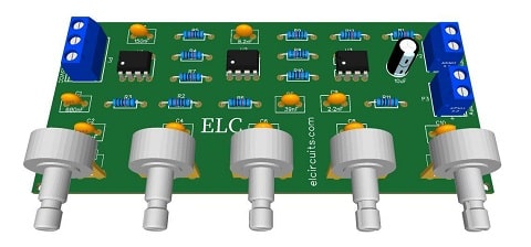
Fig. 1 - PCB 3-Band Active Equalizer Circuit with LF353 IC


This three-band active graphic equalizer circuit is an active filter set for three basic audio equalization ranges, bass, mid and treble. The circuit is based on the LF353 operational amplifier integrated circuit.

The LF353 is a two-input JFET operational amplifier with an internally compensated input offset voltage. The JFET input device provides wide bandwidth, low input bias currents and offset currents.

You might also be interested in:

Features

  • Internally Trimmed Offset Voltage: 10 mV
  • Low Input Bias Current: 50pA
  • Low Input Noise Voltage: 25 nV/√Hz
  • Low Input Noise Current: 0.01 pA/√Hz
  • Wide gain bandwidth: 4 MHz
  • High slew rate: 13V / μs
  • Low Supply Current: 3.6 mA
  • High Input Impedance: 1012Ω
  • Low Total Harmonic Distortion : 0.02%
  • Low 1/f Noise Corner: 50 Hz
  • Fast Settling Time to 0.01%: 2 μs

The equalizer circuit.

The 3-band Equalizer use a Integrated Circuits operational amplifier LF353, and the capacitors determine the frequencies, the higher their capacitance, the lower the cutoff frequencies.

The proposed equalizer is a 2-octave graphic equalizer with a 3-band circuit, the cut-off frequencies are at: 150Hz, 1kHz and 12kHz.

This circuit was assembled with LF353, but nothing prevents you from using other replacement pin compatible ICs, such as: LM1558RC4558, LM358 etc.
 
The recommended supply voltage is between ±11V and ±15V, but note that the maximum voltage IC supports is ±18V. The IC consumption current is 6.5mA maximum, and 3.6mA average.

The IC has two internal amplifiers, we get a amplifier for each frequency and the last one for the final amplification of the entire circuit. In Figure 2 below, the pinout and configuration of the LF353 integrated circuit is shown.

Fig. 2 - Pinout IC LF353

In Figure 3 below, we show the complete 3-band equalizer circuit, and that you can download the files in option; Download files below at the bottom of the page.

Fig. 3 - Schematic Diagram 3-band Active Equalizer Circuit with LF353 IC

Components List

  • U1 .............. Integrated circuit LF353

  • R1, R2, R5, R6 ... 10K resistor (brown, black, orange, gold)
  • R3, R7 ................ 3.6K resistor (orange, green, red, gold)
  • R4, R8 ................ 1.8K resistor (brown, gray, red, gold)

  • C1 ...................... 4.7uF electrolytic capacitor
  • C2 ...................... 1uF electrolytic capacitor
  • C3 ...................... 50nF polyester capacitor 
  • C4, C6 ............... 5nF polyester capacitor
  • C5 ...................... 22nF polyester capacitor

  • VR1 .................... 47K Potentiometer 
  • VR2, VR3 .......... 100K Potentiometer 
  • VR4 .................... 500K Potentiometer 

  • P1  ....................... Screw Terminal Type 5mm 3-Pin Connector
  • P2, P3 .................. Screw Terminal Type 5mm 2-Pin Connector
  • Others .................. PCB, tin, wires, etc.

Download

We provide the files with the PCB, the schematic, the PDF, GERBER and JPG, PNG and provide a direct link for free download and a direct link, "MEGA".

Click on the direct link to download the files: Layout PCB, PDF, GERBER, JPG

If you have any questions, suggestions or corrections, please leave them in the comments and we will answer them soon.

Subscribe to our blog!!! Click here - elcircuits.com!!!

My Best Regards!!!


Monday, October 18, 2021

5-Band Graphic Equalizer Circuit using LF353 IC + PCB

Fig. 1 - 5-Band Equalizer Circuit with LF353 IC

This 5 Band graphic equalizer circuit is based on the eight pins operational amplifier LF353 integrated circuit.

The LF353 is a two-input JFET operational amplifier with an internally compensated input offset voltage. The JFET input device provides wide bandwidth, low input bias currents and offset currents.

You might also be interested in:

Features

  • Internally trimmed compensated voltage: 10mV
  • Low input bias current: 50pA
  • Wide gain bandwidth: 4 MHz
  • High slew rate: 13V / μs
  • High input impedance: 1012Ω

The equalizer circuits

The proposed equalizer is a 2-octave graphic equalizer with a 5-band circuit, the cut-off frequencies are at: 50Hz, 200Hz, 800Hz, 3.2kHz and 12kHz.

This circuit was assembled with LF353, but nothing prevents you from using other replacement ICs, such as: LM1458, RC4558, etc.

The Power Supply

The power supply used for this circuit is symmetric, i.e.: +15V | 0V | -15V, with a direct current voltage DC.

The recommended supply voltage ranges between ±11V and ±15V, but note that the maximum voltage supported by the IC is ±18V.
The consumption current of the IC is 6.5mA maximum and 3.6mA on average.

The Circuit

The 5-band Equalizer uses three Integrated Circuits operational amplifier LF353, and the capacitors determine the frequencies, the higher their capacitance, the lower the cutoff frequencies.

Each IC has two internal amplifiers, we get an amplifier for each frequency and the last one for the final amplification of the entire circuit. In Figure 2 below, the pinout and configuration of the LF353 integrated circuit is shown.
Fig. 2 - Pinout IC LF353


In Figure 3 below, we show the complete 5-band equalizer circuit, and that you can download the files in option; Download files below at the bottom of the page.
Fig. 3 - Schematic Diagram 5-band Equalizer Circuit with LF353 IC

Components List

  • U1, U2, U3 .... LF353 Integrated circuit

  • R1  ................. 47K resistor (yellow, purple, orange, gold)
  • R2 to R11 ...... 10K resistor (brown, black, orange, gold)
  • R12 ................ 100K resistor (brown,  black, yellow, gold)

  • C1 ................... 680nF polyester capacitor
  • C2, C3 ............ 150nF polyester capacitor 
  • C4 ................... 33nF polyester capacitor
  • C5 ................... 39nF polyester capacitor
  • C6, C7 ............ 8.2nF polyester capacitor
  • C8, C9 ............ 2.2nF polyester capacitor
  • C10 ................. 470pF polyester capacitor
  • C11 ................. 4.7uF electrolytic capacitor

  • VR1 to VR5 ... 47K Potentiometer 

  • P1  .................. Screw Terminal Type 5mm 3-Pin Connector
  • P2, P3 ............. Screw Terminal Type 5mm 2-Pin Connector
  • Others ............. PCB, tin, wires, etc.

Download

We provide the files with the PCB, the schematic, the PDF, GERBER and JPG, PNG and provide a direct link for free download and a direct link, "MEGA".

Click on the direct link to download the files: Layout PCB, PDF, GERBER, JPG

If you have any questions, suggestions or corrections, please leave them in the comments and we will answer them soon.

Subscribe to our blog!!! Click here - elcircuits.com!!!

My Best Regards!!!

Monday, September 6, 2021

1W Amplifier for Stereo Headphone using TDA2822 IC + PCB

Fig. 3 - PCB - 1W Amplifier for Stereo Headphone with IC TDA2822M

Simple headphone amplifier with few external components that is easy and inexpensive to assemble. This IC is designed for amplifying portable devices such as CD players, portable radios, small speakers, etc.

First of all, we will use it to amplify the audio signal for headphones, that is, we will build a headphone amplifier, whether to listen to music from a mobile phone, connect instruments to study, such as electric guitar, bass guitar, ukulele, guitar, or any other audio signal that needs to be amplified. 

You might also be interested in:

The main component is the TDA2822, a monolithic integrated circuit in an 8-pin lead  Mini-dip package. It is intended for use as a dual audio power amplifier in portable audios.

FEATURES

  • Dual Low-voltage power amplifier 
  • Supply voltage down to 1.8V 
  • Low crossover distortion                                
  • Low quiescent current z Bridge or stereo configuration
The maximum input voltage of this IC is 15V DC, so do not apply more than 15V to the IC. The circuit volume can be adjusted using a 47K doble potentiometer is used in the circuit.

The schematic diagram circuit of the 1W audio Amplifier for Stereo Headphone with IC TDA2822M  is shown in Figure 2 below.

Fig. 2 - 1W Amplifier for Stereo Headphone with IC TDA2822M

Material List

  • IC1 .................. Integrated Circuits TDA2822M
  • R1, R2 ............ 1/4W / 4.7Ω Resistor 
  • C1, C2 ............ 1uF - 25V Electrolytic capacitor 
  • C3, C4, C5 ..... 100uF - 25V Electrolytic Capacitor 
  • C6, C7 ............ 0.1uF Polyester capacitor
  • J1, J2 .............. 3.5mm Audio Female Jack Connector 
  • VR1 ................ 47KΩ  Double Potentiometer
  • P1 ................... Connector 2 screw terminal 5mm 2 Pins
  • Others ............ Wires, Solders, pcb, etc.

We offer for download the necessary materials for those who want to assemble with PCI - Printed Circuit Board, the files in PNG, PDF and GERBER files for those who want to send for printing.

Download:


If you have any questions, suggestions or corrections, please leave them in the comments and we will answer them soon.

Subscribe to our blog!!! Click here - elcircuits.com!!!

My Best Regards!!!