70W Stereo Hi-Fi Amplifier using Dual TDA2050 ICs + PCB

Build a high-fidelity stereo sound amplifier with 70W of real power using the classic TDA2050 IC. A robust project with internal protections and exceptional sound quality for audio enthusiasts.
If you’ve already assembled our 35W HI-FI amplifier with a single TDA2050, you know what this integrated circuit is capable of. The audio quality is impressive for its cost-benefit ratio. But what if you double the bet?
In my bench tests, I realized that many want more power without giving up simplicity. The answer lies precisely in duplicating a good circuit. In today’s post, we’ll get straight to the point: you will build a 70W RMS HI-FI stereo amplifier using two TDA2050 integrated circuits. This is the logical evolution of the previous project, maintaining fidelity and doubling the power for larger environments.
🎯 Why Choose the TDA2050 for a 70W Project?
The TDA2050 is one of the most reliable and popular audio amplifier integrated circuits for DIY projects. Experience has shown me that it achieves an almost perfect balance between performance, cost, and ease of use. Let’s demystify it.
What is the TDA2050 Integrated Circuit?
The TDA2050 is a class AB monolithic audio power amplifier. In simple terms, it’s a chip that contains all the transistors and circuits necessary to amplify a weak audio signal, coming from a cell phone or computer, and convert it into enough power to move speakers in a crystal clear manner.
Its numbers are impressive: it provides up to 35W RMS at 4 Ohms and 32W RMS at 8 Ohms with very low total harmonic distortion (THD), generally below 0.5% at medium powers. This low distortion is the secret of the “clean” and “faithful” sound that characterizes a HI-FI equipment.
The Protections That Make the Difference
Here is the secret to the TDA2050’s durability. Unlike discrete transistors that burn out with a mistake, this IC comes with built-in protection systems. Think of them as an ABS brake system and airbags for your amplifier.
- Output Short-Circuit Protection: If you accidentally touch the speaker wires, the circuit instantly limits the current, protecting the internal output transistors. It’s not just a fuse; it’s an intelligent limitation of peak power.
- Automatic Thermal Shutdown: This is my favorite. The internal junction of the chip cannot exceed 150°C. If the heat sink is too small for the task or the environment is very hot, the circuit automatically reduces power to cool down, without damage. It allows using heat sinks with smaller safety margin, saving space and cost.
These protections make this project foolproof for beginners and extremely robust for continuous use.
🔌 Stereo Circuit Schematic Diagram
The heart of this project is a classic and proven circuit, duplicated for both channels (left and right). If you’ve already assembled the 35W amplifier, you’ll see that it’s exactly the same design, replicated. This is the beauty: master one, master both.
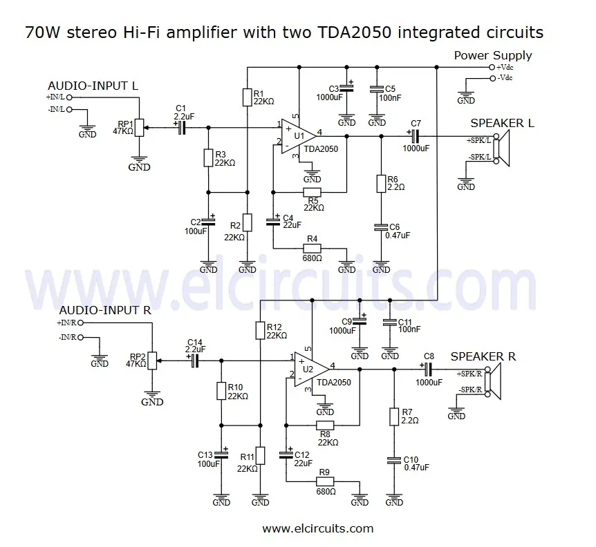
The circuit is elegant in its simplicity. Each channel uses the TDA2050 in its typical fixed gain configuration (about 30dB), defined by the feedback resistors. The input capacitors and in the feedback loop ensure frequency response and block DC voltage. The assembly is straightforward, and the chance of error is minimal if you follow the component list.
🛠️ Component List for Assembly
Use this list as your definitive shopping list. I recommend separating the components by channel to facilitate assembly. The quality of electrolytic and polyester capacitors directly influences the quality of the final sound.
-
Integrated Circuits:
- U1, U2 – TDA2050 Integrated Circuit (2 units)
-
Resistors (1/4W, 5%):
- R1, R2, R3, R5, R8, R10, R11, R12 – 22KΩ (8 units)
- R4, R9 – 680Ω (2 units)
- R6, R7 – 2.2Ω (2 units)
-
Capacitors:
- C1, C14 – 2.2µF 25V Electrolytic (2 units)
- C2, C15 – 100µF 25V Electrolytic (2 units)
- C3, C7, C8, C9 – 1000µF 35V Electrolytic (4 units – pay attention to polarity)
- C4, C12 – 22µF 25V Electrolytic (2 units)
- C5, C11 – 100nF (104) Polyester (2 units)
- C6, C10 – 0.47µF (474) Polyester (2 units)
-
Controls and Connectors:
- RP1, RP2 – 47KΩ Logarithmic (Audio) Potentiometer (2 units)
- P1, P3 – 3-Pin Screw Terminal Connector (for audio input)
- P2 – 2-Pin Screw Terminal Connector (for power supply)
- Materials: Printed Circuit Board (PCB), Heat Sink for 2 TDA2050, Wires, Solder, Metal Case, Knobs, etc.
🖨️ Printed Circuit Board (PCB)
To ensure the best audio performance and minimize noise, a good PCB layout is not just recommended, it’s essential. Short traces for audio signals, a solid ground plane and the correct placement of filter capacitors make all the difference between an amplifier “that works” and one that “sounds professional”.
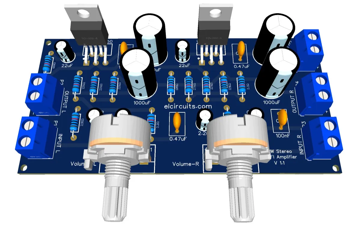
📥 Download Files for Manufacturing
We designed the PCB to meet both hobbyists who will etch their board at home and those who want to order a professional board. The files are ready to send to services such as JLCPCB, PCBWay or any other factory.
Download PCB Files (GERBER, PDF, PNG)
The package includes: GERBER Files (for manufacturing), PDF in layers (for manual transfer) and high-resolution PNG images (for visualization).
🤔 Frequently Asked Questions (FAQ)
To ensure your project is a success, we’ve compiled some of the most common questions on this topic. Check them out!
What is the real output power of this amplifier with a ±18V supply? 🔽
With a symmetrical supply of ±18V and 4 Ohm speakers, each channel will deliver about 35W RMS, totaling 70W RMS in the stereo system. With 8 Ohm speakers, the power per channel drops to approximately 24W RMS. These values are with very low distortion (THD < 0.5%).
Can I use a non-symmetrical supply (only +V and GND) in this project? 🔽
No. The TDA2050 circuit was designed to operate with symmetrical supply (e.g., +18V, GND, -18V). Using a simple supply (like 12V or 24V with a single terminal) will not work. You will need a transformer with center tap or a symmetrical switching supply.
What is the ideal size of the heat sink for the two TDA2050? 🔽
For continuous use at high volume, I recommend an aluminum heat sink with thermal resistance less than 2°C/W per chip. A single extruded aluminum block about 10cm long, 5cm high and 3-4cm fins is usually sufficient. Use quality thermal paste and isolate the screws with mica or silicone bushings.
Can I replace the electrolytic capacitors with other values? 🔽
Some capacitors have margin, others are critical. You can increase the capacitance of the power supply filter electrolytics (C3, C7, C8, C9) to 2200µF or more, which improves the response to low frequencies at high volume. However, the capacitors in the feedback loop (C6, C10) and decoupling (C5, C11) should maintain their values to ensure the circuit’s stability and correct frequency response.
💡 Fresh Ideas for Your Next Project
Did you enjoy this project? Then you’ll love exploring other circuits we’ve prepared. Each one with its unique features and ideal applications!
- 170W AB Class Bridge Mode Amplifier using TDA7294 IC + PCB
- High Fidelity 14W – 12V Power Amplifier using TDA2030 IC + PCB
- 24W Stereo Hi-Fi Audio Amplifier using TDA2616 + PCB
- HI-FI 120W RMS Amplifier Circuit using LM4780 IC + PCB
- 4 x 50W High Power Amplifier, 14.4V – IC TDA7563A + PCB
- HI FI 32W Audio Amplifier – TDA2050 – Simple PS + PCB
- 180W RMS 4-Channel Amplifier with TDA7386 + PCB
- 320W Power Audio Amplifier, Powered with 14.4V – 2Ω with IC TDA7560 + PCB
- 100W RMS Audio Amplifier IC TDA7294 + PCB
- 200W RMS Stereo Power Amplifier with IC STK4231II + PCB
🎵 Conclusion: Your Path to High-Fidelity Sound
Building this 70W stereo amplifier with TDA2050 is more than an electronics project; it’s a rite of passage for any audio enthusiast. You will not only have powerful and quality equipment, but also the deep knowledge of how it works, piece by piece.
The robustness of the TDA2050’s internal protections, combined with the simplicity of the circuit, makes this an ideal project for beginners seeking a challenge and veterans who appreciate reliable results. The sound is clear, dynamic and with enough authority for a medium room or even a small event.
Ready to get started? Download the PCB files, gather the components and start your assembly. When you turn it on and listen to the first song, you’ll understand why the TDA2050 is a timeless classic.
👋 Share Your Experience! In my years of mentoring, I’ve learned that community makes the difference. Finished the assembly? Had any questions? Leave a comment below sharing your results or questions. Your journey can inspire and help other builders. And don’t forget to check out our other amplifier projects for your next challenge!
✨ Our Gratitude and Next Steps
We sincerely hope this guide has been useful and enriching for your projects! Thank you for dedicating your time to this content.
Your Feedback is Invaluable:
Have any questions, suggestions, or corrections? Feel free to share them in the comments below! Your contribution helps us refine this content for the entire ElCircuits community.
If you found this guide helpful, spread the knowledge!
🔗 Share This GuideBest regards,
The ElCircuits Team ⚡
 Português
 Español
