Português
 Español
NodeMCU ESP8266: Pinout and Features!
The NodeMCU ESP8266 board is one of the most popular development platforms for Internet of Things (IoT) and home automation projects. Based on the ESP8266 microcontroller (ESP-12E Module), this board combines built-in Wi-Fi connectivity with a user-friendly interface for rapid prototyping, making it an ideal choice for both beginners and experienced developers.
In this comprehensive guide, we’ll explore in detail the pinout of the NodeMCU ESP8266, analyzing each pin, its functions, and limitations. Understanding the pinout is essential to fully leverage the potential of this board in your projects, avoiding damage and ensuring correct operation of your applications.
Pinout Diagram
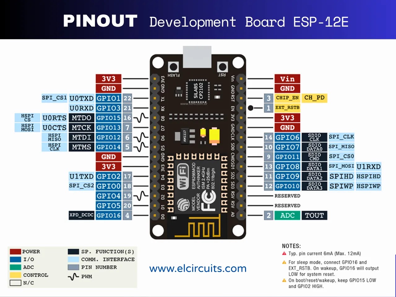
Pinout diagram of NodeMCU ESP8266 development board.
I/O (Input/Output) Pin Table
| Pin on Board | GPIO (Chip) | Main Functions | Critical Notes / Default State |
|---|---|---|---|
| D0 | GPIO16 | I/O, Wake up from deep sleep | Does not support PWM, I2C or I2S. Can be used to wake from deep sleep. |
| D1 | GPIO5 | I/O, SCL (I2C) | Frequently used as SCL for I2C communication. |
| D2 | GPIO4 | I/O, SDA (I2C) | Frequently used as SDA for I2C communication. |
| D3 | GPIO0 | I/O, Flash mode select | Must be LOW during boot to enter flash mode. Internal pull-up. |
| D4 | GPIO2 | I/O, LED onboard | Connected to the onboard blue LED. Must be HIGH during boot. |
| D5 | GPIO14 | I/O, SCLK (SPI) | Frequently used as SCLK for SPI communication. |
| D6 | GPIO12 | I/O, MISO (SPI) | Frequently used as MISO for SPI communication. |
| D7 | GPIO13 | I/O, MOSI (SPI) | Frequently used as MOSI for SPI communication. |
| D8 | GPIO15 | I/O, SS (SPI) | Must be LOW during boot. Internal pull-down. |
| RX | GPIO3 | UART RX | UART receiver. Can be used as a general I/O pin. |
| TX | GPIO1 | UART TX | UART transmitter. Must be HIGH during boot for debug output. |
| A0 | ADC0 | Analog Input | 10-bit resolution (0-1023). Maximum voltage of 3.3V. |
Power and Control Pin Table
| Pin on Board | Name | Function | Technical Description |
|---|---|---|---|
| VIN | Vin | Power Input | Accepts 7-12V DC voltage. Internally regulated to 3.3V. |
| 3V3 | 3.3V | Power Output | Provides 3.3V regulated from VIN or USB. Maximum of 600mA. |
| GND | Ground | Ground | Ground reference for the circuit. |
| EN | Enable | Chip Enable | Activates the ESP8266 when HIGH. Internal 10kΩ pull-up. |
| RST | Reset | System Reset | Resets the ESP8266 when LOW. Internal 10kΩ pull-up. |
Schematic Diagram
The schematic diagram of the NodeMCU ESP8266 reveals the internal organization of components and connections on the board. This schematic is essential to understand how the different modules interact and how power is distributed throughout the circuit.

Fig. 2 – Schematic Diagram NodeMCU ESP8266
To view the complete schematic of the ESP8266 module, including detailed pinout, we recommend accessing the official Espressif documentation. The document contains complete and up-to-date technical information about the module’s hardware. Click here to access the schematic on the official Espressif website.
Summary of Electrical Characteristics and Limitations
-
Operating Voltage: The ESP8266 operates internally with
3.3V. All GPIO pins work with this voltage and are not 5V tolerant. - Power Supply: The board can be powered via USB (5V) or through the VIN pin (7-12V), being internally regulated to 3.3V.
-
Current per GPIO: Each GPIO pin can provide a maximum of
12mAof continuous current. It is recommended not to exceed 10mA to ensure the longevity of the chip. -
Boot Pins: The pins
GPIO0,GPIO2andGPIO15have specific states during boot and must be carefully managed. -
USB-Serial Converter: Most NodeMCU boards use the
CH340GorCP2102chip for USB-Serial communication, allowing programming and debugging via USB port. -
ADC: Has only one analog input pin (
A0) with 10-bit resolution (0-1023) and range of 0-3.3V. - Memory: The ESP-12E module has 4MB of flash memory, allowing storage of programs and data.
- Wi-Fi: Integrates Wi-Fi 802.11 b/g/n connectivity with support for WPA/WPA2, operating in station mode, access point or both simultaneously.
Understanding the pinout and electrical characteristics of the NodeMCU ESP8266 is essential for developing robust and functional projects. This guide serves as a quick reference for consultations during development, helping to avoid common errors such as pin overload, incorrect boot configurations or damage due to inadequate voltage. Always remember to consult the official documentation for more detailed and specific information about your version of the board.
🤔 Frequently Asked Questions (FAQ): About the NodeMCU ESP8266 Pinout
To ensure your project is a success, we’ve compiled some of the most common questions about this development board. Check it out!
❓ Can I power the NodeMCU ESP8266 directly with 5V on the GPIO pins?🔽
No, the ESP8266 GPIO pins are not 5V tolerant and operate exclusively with 3.3V. Applying 5V to any GPIO pin can permanently damage the microcontroller. If you need to interact with 5V devices, use a logic level converter to ensure chip protection.
❓ How do I put the NodeMCU in flash mode for programming?🔽
To put the NodeMCU in flash mode, you need to keep the GPIO0 (D3) pin at LOW level during the boot process. This can be done by pressing the FLASH button (which connects GPIO0 to GND) while pressing and releasing the RESET button. Keep the FLASH button pressed until the programming process starts.
❓ How many PWM pins can I use simultaneously on the NodeMCU?🔽
The NodeMCU ESP8266 supports PWM on almost all GPIO pins, except on GPIO16 (D0). However, the PWM implementation on the ESP8266 is software-based, which means the precision may vary depending on the number of active PWM channels and the processing load. For critical applications that require high precision, consider using dedicated hardware or limiting the number of simultaneous PWM channels.
❓ What is the maximum current that the NodeMCU can provide to external components?🔽
Each individual GPIO pin can provide a maximum of about 12mA of continuous current. The total current that all GPIO pins can provide simultaneously is limited to approximately 200mA. For components that require more current, such as motors or LED strips, it is necessary to use external power supplies and suitable drive circuits, such as transistors or relays.
❓ Can I use all GPIO pins for I2C or SPI communication?🔽
Although it is technically possible to implement I2C or SPI in software on almost all GPIO pins, there are recommended standard pins for these communications. For I2C, the pins D1 (GPIO5/SCL) and D2 (GPIO4/SDA) are conventionally used. For SPI, the pins D5 (GPIO14/SCLK), D6 (GPIO12/MISO), D7 (GPIO13/MOSI) and D8 (GPIO15/SS) are the standards. Using these pins facilitates compatibility with existing libraries.
❓ How does the A0 (ADC) pin work and what is its precision?🔽
The A0 pin is the only analog input pin of the ESP8266, with 10-bit resolution (values from 0 to 1023). Its maximum input voltage is 3.3V. The precision of the ESP8266 ADC is not very high and can be affected by noise and temperature variations. For more accurate measurements, it is recommended to take multiple readings and calculate the average, or use a higher precision external ADC connected via I2C or SPI.
🔗 Explore More Amazing Projects
Did you like this project? Then you’ll love exploring other charger circuits we’ve prepared. Each with its own peculiarities and ideal applications!
✨ Our Gratitude and Next Steps
We sincerely hope this guide has been useful and enriching for your projects! Thank you for dedicating your time to this content.
Your Feedback is Invaluable:
Have any questions, suggestions, or corrections? Feel free to share them in the comments below! Your contribution helps us refine this content for the entire ElCircuits community.
If you found this guide helpful, spread the knowledge!
🔗 Share This Guide
Best regards,
The ElCircuits Team ⚡