Showing posts with label Amplifier. Show all posts

Wednesday, May 19, 2021

40W Stereo 14.4V Car Audio Power Amplifier using TDA8560Q IC + PCB

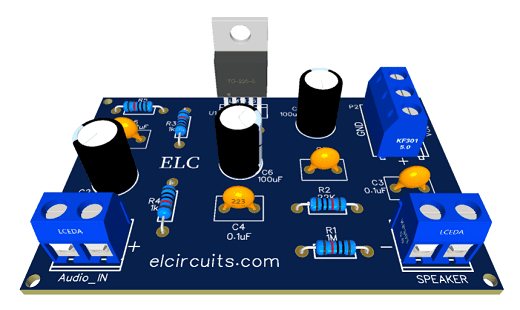
Fig. 1 - PCB 40W Stereo Car Amplifier TDA8560Q

For Portuguese Version, Click Here!

This is a super easy to build Stereo Car Audio Power Amplifier circuit, due to the number of external components being few, it makes this amplifier quite viable for those who want to build a power amplifier and super simple and quick to do.

The TDA8560Q is an integrated Class-B output amplifier in a 13-lead Single-In-Line (SIL) power package.

This Car Audio Amplifier Circuit gives an output power 2×40W / 2 Ω in BTL configuration. The device is primarily developed for car radio applications.  

The TDA8560Q contains two identical amplifiers and can be used for bridge applications. The gain of each amplifier is fixed at 40 dB. Special features of the device are as follows.

You might also be interested in:

Mode select switch (pin 11)

  • Standby: low supply current (<100 µA)
  • Mute: input signal suppressed
  • Operating: normal on condition.

Since this pin has a very low input current (<40 µA), a low cost supply switch can be applied. To avoid switch-on plops, it is advised to keep the amplifier in the mute mode during ≥100 ms (charging of the input capacitors at pin 1 and pin 13).

The schematic diagram of the Car Amplifier Circuit, is in Figure 2 below, it is a very simple circuit to build, with few external components, however, it is a very powerful circuit, which provides 80W in two 2 Ohms Speakers.

Fig. 2 - 40W Stereo 14.4V Car Audio Power Amplifier - IC TDA8560Q

The operating voltage of this circuit can vary between 6V to 18V DC, which opens the possibilities of use in amplifier for; Residential Sound, Car Stereo, Boombox, Computer Speaker, among other types of portable audio amplifiers ... Since it has a common power supply and low power voltage, this circuit amplifier is ideal for these purposes.

Components List

  • U1 ..................TDA8560Q Integrated Circuit
  • R1, R2, R3 .... 10K ohms - 1/8 W Resistor - (brown, black, orange, gold)
  • C1, C2 ........... 470nF Polyester Capacitor
  • C3 .................. 47uF - 35V Electrolytic capacitor 
  • C4 .................. 2200uF - 35V Electrolytic capacitor
  • C5 .................. 100nF Ceramic Capacitor
  • RP1, RP2 ....... 20K ohms Potentiometer 
  • JP1, JP2 .......... Female RCA Connectors to PCB
  • P1, P2, P3 ....... PCB Terminal Blocks
  • Others ............. Wires, Welds, Posts, PCB, Etc.

We are making available the files containing the PCB, the Schematic Diagram, the PDF, GERBER, and JPG, and providing a direct link to download for free in a direct link, "MEGA".

Direct link to download

Click in the link  to download the Files: PCB Layout, PDF, GERBER, JPG

If you have any questions, suggestions or corrections, please leave them in the comments and we will answer them soon.

Subscribe to our blog!!! Click here - elcircuits.com!!!

My Best Regards!!!

Sunday, April 18, 2021

300W RMS Power Amplifier - 2SC3858 and 2SA1494 Transistors + PCB

Fig. 1 - PCB 300W RMS Power Amplifier - 2SC3858 and 2SA1494 Transistors


This is a 300W RMS Power Amplifier using complementary power transistors 2SC3858 and 2SA1494, this circuit amplifier isn't so simple to building, it will be necessary to have at least a little experience in electronics.

To set up this circuit, its complexity is moderate, but, if you haven't skills in electronics circuits, we advise you not to do it, however, if you really want to do it, call someone with experience, to help you.

This amplifier has an excellent audio quality, and use four output power transistors, it reaches a sound power of 300W RMS under load of 4 ohms, powered with a symmetric power supply. You can check the schematic diagram in Figure 2 below.

Fig. 2 - Schematic 300W RMS Power Amplifier - 2SC3858 and 2SA1494 Transistors

Power Supply

The power supply consists of a symmetrical transformer 45V - 0 - 45V center tape, 6 Amperes current supply, can be used. After rectified, we will have approximately 63Vcc at the output of the symmetrical power supply .

Components list

  • Q1, Q2, Q3, Q5 ......... C1815 NPN Transistor
  • Q4 .............................. A1015 PNP Transistor 
  • Q7 .............................. TIP 42C PNP Transistor
  • Q8, Q9 ....................... 2SC3858 NPN Power Transistor
  • Q10, Q11 ................... 2SA1494 PNP Power Transistor
  • Q6 .............................. TIP41C NPN Transistor

  • D1 to D7 .................... 1N4148 diode, or equivalent diode 1N4001 
  • C1, C4 ......................... 2.2uF - 25V Electrolytic Capacitor   
  • C2 ............................... 220pF Polyester / Ceramic Capacitor 
  • C8 ............................... 100nF Polyester / Ceramic Capacitor 

  • R2, R10 ....................... 47k ohms resistor (yellow, violet, orange, gold)
  • R3, R5 ......................... 2.2k ohms resistor (red, red, red, gold)
  • R4 ................................ 270 ohms resistor (red, violet, black, gold)
  • R6, R7 ......................... 51K ohms - 1/2W resistor (green, brown, orange, gold)
  • R8, R9, ........................ 100 ohms resistor (brown, brown, black, gold)
  • R11 .............................. 470 ohms resistor (yellow, violet, brown, gold)
  • R12 .............................. 390 ohms resistor (orange, white, brown, gold)
  • R13, R14 ..................... 100 ohms - 2W resistor (brown, brown, black, gold)
  • R17, R18 ...................... 6R8 ohms - 1W resistor (blue, gray, gold, gold)
  • R15, R16, R19, R20 .... 100 ohms - 1W resistor (brown, brown, black, gold)
  • R21, R22, R23, R24 .... 0.33 ohms - 5W resistor (orange, orange, gold, gold)
  • R25 .............................. 22 ohms resistor (red, red, black gold)
  • R26 .............................. 10 ohms - 1W resistor - (brown, black, black. gold)

  • P1, P2 ....... 2 Pin - PCB Terminal Blocks - EK500V-XXP 20A - or equivalent
  • P3 ............. 3 Pin - PCB Terminal Blocks - EK500V-XXP 20A - or equivalent

  • L1 ............. 5uH - Air Core Coil 10 Turns 18AWG, 3/8" Core

  • Others ...... Loudspeaker, Wires, Solders and Etc.


For those who want to download materials such as the schematic diagram in PDF, PCB Layout,  GERBER and JPG, we are providing a direct link to download all the material.

Direct link to download

Click in the link below to download the Files: PCB Layout, PDF, GERBER, JPG

If you have any questions, suggestions or corrections, please leave them in the comments and we will answer them soon.

Subscribe to our blog!!! Click here - elcircuits.com!!!

My Best Regards!!!

Wednesday, April 7, 2021

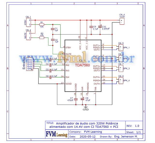
320W Power Audio Amplifier, Powered with 14.4V - 2Ω using TDA7560 IC + PCB

Fig. 1 - 320W Power Audio Amplifier - IC TDA7560


This is a simple high power amplifier circuit, with 320W divided into 4 outputs with 2Ω. This amplifier is capable of providing 50 Watts of power per channel, totaling 200W of sound power. 

But, what title does it say is 320W? That's right, the amplifier circuit with TDA7560 for which it is the base of this amplifier, was designed to provide a maximum power of 80 Watts per channel with a load of 2Ω powered by 14.4V.

Which opens up great possibilities for those who do not usually use symmetrical power supply, and you can also use this circuit as an amplifier in your car.

Since the connected car provides approximately 14.4V that serves to charge the battery, and without taking into account that this circuit may also be being powered directly by 12V, which would be when the car is off.

Output Power Settings:

For 4Ω load

VS = 13.2V - THD 10% - 4 x 25 Watts
VS = 13.2V - THD 1% - 4 x 19 Watts
VS = 14.4V - THD 10% - 4 x 30 Watts
VS = 14.4V - THD 1% - 4 x 23 Watts

For 2Ω load

VS = 13.2V - THD 10% - 4 x 45 Watts
VS = 13.2V - THD 1% - 4 x 34 Watts
VS = 14.4V - THD 10% - 4 x 55 Watts
VS = 14.4V - THD 1% - 4 x 43 Watts

Maximum Power THD> 10%

VS = 14.4V - 4Ω - 4 x 50 Watts
VS = 14.4V - 2Ω - 4 x 80 Watts

Characteristics

  • Hi-Fi Distortion Class
  • Low output noise
  • St-by function
  • Mute function
  • Auto Mute in min. Supply voltage detection
  • Supply voltage range from 8 to 18Volts
  • Low external component account:
  • Internally fixed gain (26db)
  • No external compensation
  • Without Bootstrap Enablers
  • 0.35A onboard pre-driver

Standby and Mute

The Standby and Mute installations are both compatible with CMOS, if you do not want to use a direct connection with the respective Vs pins.

You can use standard low power transistors to drive the Mute and Stand-By pins if you do not want to use the ports CMOS or even use microprocessors.

The R-C set should always be used to smooth the transitions to avoid audible transient noise. In Stand-By mode, the time constant to be assigned to achieve a transition practically free of pop-ups must be slower than 2.5V / ms.

In Figure 2 below, we have the schematic diagram of the Audio Amplifier with 320W Power, powered with 14.4V with IC TDA7560, as we can see, it is a very simple circuit, compared to its insight, so small.

However, quite powerful, and this is great because it makes assembly a lot easier for those who do not have great experiences with electronics and also wants to participate in this excellent and incredible world of electronics.
Fig. 2 - Audio Amplifier with 320W - Powered with 14.4V with CI TDA7560

The power supply must provide a current of at least 7 Amperes. It is important to remember that the maximum supply voltage allowed by this IC is 18 Volts, if we exceed this supply voltage we can burn the Integrated Circuit.

Components List

  • CI 1 ................................ TDA7560 Integrated Circuit
  • R1 .................................. 10KΩ Resistor (brown, black, orange, gold)
  • R2 .................................. 47 KΩ Resistor (yellow, violet, orange, gold)
  • C1, C2 ........................... 1μF Ceramic capacitor / polyester
  • C3, C4, C5, C6, C9 ....... 0.1μF Ceramic / polyester capacitor 
  • C7 .................................. 470nF Ceramic / polyester capacitor 
  • C8 .................................. 47μF - 25V Electrolytic capacitor 
  • C10 ................................ 2.200μF - 25VElectrolytic capacitor 
  • CN 1, 2, 4, 5, 6, 7, 8 ...... 2-Pin PCB Terminal Blocks - EK500V-XXP
  • CN 3 .............................. 5-Pin Card-to-Cable Connector
  • Others ............................ Printed Circuit Board, tin, wire, etc.
The PCB - Printed Circuit Board, has its dimensions of; 83.439mm width by 58.166mm depth, and, We are making available for Download the necessary materials for those who want to assemble with PCB, the files in PNG, PDF and GERBER files for those who want to send for printing.

Download:

Direct Link: PNG, PDF, GERBER files

This post is an authorized copy of our partner www.fvml.com.br. For those who want to follow step by step the assembly of this amplifier and the sound tests, you can access the video in Portuguese on the FVML Youtube channel by accessing below.

If you have any questions, suggestions or corrections, please leave them in the comments, and we will answer them soon.

Subscribe to our blog!!! Click here - elcircuits.com!!!

My Best Regards!!!

Thursday, April 1, 2021

50W RMS Audio Amplifier with IRF530 and IRF9530 Mosfet + PCB

Fig. 1 - PCB 50W Audio Amplifier

For Portuguese version, click here!

This circuit amplifier is very simple to building, however, although simple, it has an excellent audio quality, and with just two output transistors, it reaches a sound power of 50W RMS under load of 8 ohms, which is enough for a great home sound system, or for speakers for musical instruments ... the possibilities are endless.

The first stage of the amplifier is a differential amplifier based on the transistors Q1 and Q2. Capacitor C2 is the input DC decouple, R1 limits the input current and capacitor C1 deflects unwanted high frequencies.

You might also be interested in:

The second stage is the drive stage composed of the transistor Q3 BC546, which supplies the output power stage, and the transistor Q4 is the bias regulating transistor, which, through the PR1 trimpot, adjusts the quiescent current in the transistors.

The output stage is a complementary push-pull stage based on the IRF530 and IRF9530 MOSFETs. The output is coupled to the speaker using the L1 inductor

The network composed in series by hairs, resistor R14 and capacitor C5, is intended to reduce output noise. And Capacitors C6 and C7 are power supply voltage filters. 

For coil L1: Wrap 12 turns of enameled copper wire in a 1cm diameter without core.

A Heatsink is required for MOSFETs. That should have the average dimensions of 8x4x4 inches will already work without problems.

You can check the schematic diagram in Figure 2 below.

Fig. 2 - 50 Watt Amplifier Circuit Diagram

Power Supply

The power supply consists of a symmetrical transformer 35Vcc - 0 - 35V center tape, with a current of 3 Amperes, a lower current, up to 2 Amperes minimum, can be used, which will play without any problems. 

Nothing prevents you from using a higher or lower voltage, as this amplifier has a tolerance for the supply voltage, and can normally play "with small attenuations in the output power" with voltages ranging from 27V to 40V without too many problems.

It also has great stability and we can use, if you have, a SMPS power supply, and this is clear with Center-Tape, that is to say a power supply with central socket.

Component List

  • Q1, Q2 ................ 2N3906 Transistor (or BC558, A733)
  • Q3, Q4 ................ 2N3904 Transistor (or BC548)
  • Q5 ....................... IRF9530P Mosfet P Transistor
  • Q6 ....................... IRF530P Mosfet N Transistor

  • D1 ....................... 1N4007 Diode 

  • C1 ....................... 220pF ceramic / polyester capacitor  
  • C2, C3, C4 .......... 47uF - 35V electrolytic capacitor 
  • C5 ....................... 68nF ceramic / polyester capacitor 
  • C6, C7 ................ 470uF - 50V electrolytic capacitor 

  • R1, R8 ................ 4.7k ohms resistor (yellow, violet, red, gold)
  • R2, R7 ................ 47k ohms resistor (yellow, violet, orange, gold)
  • R3 ....................... 560 ohms resistor (green, blue, brown, gold)
  • R4 ....................... 15k ohms resistor (brown, green, orange, gold)
  • R5 ....................... 1.2k ohms resistor (brown, red, red, gold)
  • R6 ....................... 2.2k ohms resistor (red, red, red, gold)
  • R9 ....................... 10k ohms resistor (brown, black, orange, gold)
  • R10 ..................... 820 ohms resistor (gray, red, brown, gold)
  • R11, R12 ............ 2.7k ohms resistor (red, violet, red, gold)
  • R13, R14 ............ 680 ohms resistor (blue, gray, brown, gold)
  • R15 ..................... 10 ohm - 3W resistor - (brown, black, black. gold)

  • L1 ........................ 5uH - Air Core Coil 10 Turns 18AWG, 3/8" Core

  • RP1 ..................... 1K ohms variable resistor - Trimpot 

  • Others ................. Loudspeaker, Wires, Solders and Etc.

For those who want to download materials such as the schematic diagram in PDF, PCB Layout,  GERBER and JPG, we are providing a direct link to download all the material.

Direct link to download

Click in the link below to download the Files: PCB Layout, PDF, GERBER, JPG

If you have any questions, suggestions or corrections, please leave them in the comments and we will answer them soon.

Subscribe to our blog!!! Click here - elcircuits.com!!!

My Best Regards!!!

Thursday, March 25, 2021

100W RMS Audio Amplifier using TDA7294 IC + PCB

Fig. 1 - Printed Circuit Board Amplifier 100W with TDA7294


We'll assemble an excellent power amplifier, with excellent sound quality, with 100W RMS output power, with symmetrical power supply. The circuit has a wide range in the supply voltage, and we will be providing the printed circuit board for you to download.

Integrated Circuit

The TDA7294 is an Integrated Circuit with Class AB audio output, it has its Multiwatt encapsulation. It was specifically designed for high quality sound applications, such as: home micro-systems, guitar cubes, high-end televisions. 

Thanks to the wide voltage range and the high current capacity, it's able to provide the highest power in loads of 8 ohms or 4 ohms, even with low supply voltage input, with high voltage rejection circuit.

The built-in locking function with activation delay simplifies remote operation, avoiding noisy changes when pressing the On/Off button.

Characteristics

  • Wide range of supply voltage (± 10V to ± 40V)
  • DMOS output amplification step
  • High Output Power (Musical 100W)
  • Mute and Stand-by functions
  • Very low harmonic distortion
  • Short circuit protection
  • Thermal protection with automatic shutdown

The layout of the schematic diagram is just below in Figure 2, for which we have the entire configuration of the amplifier with TDA7294.
Fig. 2 - Schematic diagram 100W RMS Audio Amplifier IC TDA7294

List of materials

  • U1 .................. Integrated Circuit TDA7294
  • R1, R3, R4 .... Resistor 22K (red, red, orange, gold)
  • R2 ................. Resistor 680Ω (blue, gray, brown, gold)
  • R5 ................. 10K resistor (brown, black, orange, gold)
  • C1 .................. Electrolytic capacitor 1.5μF - 35V
  • C2, C3 ........... Electrolytic capacitor 22μF - 63V
  • C4, C5 ........... Electrolytic capacitor 10μF - 63V
  • P1, P3............. 2-Pin Card-to-Cable Connector
  • P2 .................. 3-Pin Card-to-Cable Connector
  • Others ............ Printed Circuit Board, tin, wire, etc.

Power supply

The power supply must be at least 5 AmperesSymmetrical, with good filtration, with a minimum voltage of 10 Volts and a maximum of 40 Volts

Knowing that using the minimum voltage, you will not reach the maximum power of the amplifier, because it needs a higher voltage to supply the declared power.

In this amplifier model, is used a Symmetric Power Supply type, that is; power [+ VCC GND | -VCC].

Download

We are making available for download the necessary materials for those who want to assemble with the PCB - Printed Circuit Board, the files in PNG, PDF and GERBER files, for those who want to send for printing.

Direct link to download

Click in the link below to download the Files: PCB Layout, PDF, GERBER

If you have any questions, suggestions or corrections, please leave them in the comments and we will answer them soon.

Subscribe to our blog!!! Click here - elcircuits.com!!!

My Best Regards!!!

Saturday, March 20, 2021

100W RMS Power Amplifier using 2 NPN 2SC5200 Output Transistors + PCB

Fig. 1 - 100W RMS Power Amplifier using 2 NPN 2SC5200 Output Transistors + PCB

For Portuguese version, click here!

We usually have amplifiers with complementary outputs on most amplifier designs, and in a vast majority of amplifiers, it's quite normal to use the complementary NPN 2SC5200 transistors in conjunction with the PNP 2SA1943.

This type of amplifier is very common and good quality, because these transistors are specific for high fidelity amplification.

You might also be interested in:

We'll build an amplifier circuit that uses the same concepts as two output transistors, but we will use two NPN 2SA5200 output transistors. Which is very interesting for those who like to test other types of transistors to evaluate the quality, distortions, powers. Etc.

The schematic diagram is in Figure 2 below, it is a simple amplifier, it has a satisfactory quality.

Fig. 2 - 100W RMS Power Amplifier with 2 NSC 2SC5200 Transistors at Output

Power Supply

The power supply consists of a symmetrical transformer 32V - 0 - 32V center tape, with a current of 5 Amperes, a lower current, up to 3 Amperes minimum, can be used, which will play without any problems.

Nothing prevents you from using a higher or lower voltage, as this amplifier has a tolerance for the supply voltage, and can normally play “with small attenuation in the output power” with voltages ranging from 18V to 55V without too many difficulties.

It also has great stability, and we can use, if you have, a SMPS power supply, and this is clear with Center-Tape, that is to say a power supply with central socket.

Component List

  • Q1, Q2 ............... Transistor A733
  • Q3, Q4 ............... TIP41C transistor
  • Q5 ...................... TIP42C transistor
  • Q6, Q7 ............... 2SC5200 Power Transistor

  • D1, D2, D3 ........ Diode 1N4007

  • C1 ....................... 0.47uF Polyester capacitor 
  • C2, C4, C5 .......... 47uF - 63V electrolytic capacitor 
  • C3 ....................... 100nF ceramic / polyester capacitor 
  • C6 ....................... 150pF ceramic / polyester capacitor 
  • C7, C8 ................ 1nF ceramic / polyester capacitor

  • R1 ....................... 22k ohms resistor (red, red, orange, gold)
  • R2 ....................... 15k ohms resistor (brown, green, orange, gold)
  • R3, R7 ................. 680 ohms resistor (blue, gray, brown, gold)
  • R4 ....................... 33 ohms resistor (orange, orange, black, gold)
  • R5 ....................... 560 ohms - 1W resistor (green, blue, brown, gold)
  • R6 ....................... 56k ohms resistor (green, blue, orange, gold)
  • R8, R9 ................ 4.7k ohms resistor (yellow, violet, red, gold)
  • R10 ..................... 10 ohm resistor - (brown, black, black. gold)
  • R11 ..................... 120 ohms - 1W resistor (brown, red, brown, gold)
  • R12, R13 ............ 100 ohms - 1W resistor (brown, black, brown, gold)
  • R14, R15 ............ 0.47 ohms - 5W resistor (yellow, violet, silver, gold)

  • Others ................. PCB, Heat Sink, Loudspeaker, Wires, Solders, Etc.

For those who want to download materials such as the schematic diagram in PDF, PCB Layout,  GERBER and JPG, we are providing a direct link to download all the material.

Direct link to download

Click in the link below to download the Files: PCB Layout, PDF, GERBER, JPG

If you have any questions, suggestions or corrections, please leave them in the comments and we will answer them soon.

Subscribe to our blog!!! Click here - elcircuits.com!!!

My Best Regards!!!


Friday, March 12, 2021

Simple 3 Transistors Power Amplifier push a 600W RMS Subwoofer + PCB

Fig. 1 - Simple 3 Transistors Power Amplifier PCB


This is a simple amplifier that uses only 3 transistors, and has the ability to push a 600W RMS Subwoofer speaker with great mastery.

The circuit is quite simple, and easy to assemble, we took this circuit from our Brazilian partner FVM Learning, and this is their direct link www.fvml.com.

This mini amplifier was tested in two stages, one with 24V, with a non-symmetrical power supply, and in 30V also with non-symmetrical power, the result you can watch in the original video at the end of this post.

You might also be interested in:

The Amplifier Circuit

The amplifier circuit is very simple to be arranged in figure 2 just below, it is divided into two stages: 

  • The first stage is the pre-amplification and at the same time used as a drive to boost the output stage. It is formed by a transistor medium power the BD139, which supports a voltage of up to 80V and a current of 1.5A with 12.5 W of power, according to the Datasheet of the same.

  • The second is the power stage, which is formed by the complementary transistors NPN - 2SC5200 and the PNP - 2SA1943 transistor, with 100W of power and high fidelity, whose collector current supported is 15 Amps.
Fig. 2 - Simple 3 transistors Power Amplifier schematic diagram

Note

Place the power transistors in a heat sink, especially if you are going to apply a voltage greater than 20V and use the amplifier continuously, they will heat up.

Component List

  • T1 ---------- NPN 2SC5200 Power complementary transistor
  • T2 ---------- PNP Complementary Power Transistor 2SA1943
  • T3 ---------- NPN BD139 transistor

  • D1, D2 ----- Diode 1N4007

  • C1 ---------- Electrolytic capacitor 2.200uF - 63V
  • C2 ---------- Electrolytic capacitor 4.7uF - 25V

  • R1, R2 ----- Resistor 0.22 ohms - 5W - (red, red, silver)
  • R3 ---------- Resistor 1k ohms - (brown, black, red)
  • R4 ---------- Resistor 100k ohms - (brown, black, yellow)

  • P1 ---------- 10K ohm potentiometer

  • Others ----- Wires, Welds and Etc.

Watch the original video of the FVML channel of the tests, and the assembly step by step, and be surprised !!!!


We are offering to download the link with the printed circuit board printing files, they are; Gerber, PDF layout, PNG, all the files with a direct link to Mega.

Direct link to download

Click in the link below to download the Files: PCB Layout, PDF, GERBER
Click Here!!!

If you have any questions, suggestions or corrections, please leave them in the comments and we will answer them soon.

Subscribe to our blog!!! Click here - elcircuits.com!!!

My Best Regards!!!

Friday, February 19, 2021

200W RMS Stereo Power Amplifier using STK4231II IC + PCB

Fig. 1 - PCB 200W RMS Stereo Power Amplifier IC STK4231II


This audio amplifier circuit is a HI-FI two-channel 100w OCL High Power Stereo Audio Amplifier based on the STK4231II IC.

STK4231 is a Thick film hybrid IC two-channel  100W min AF Power Amp, manufactured by SANYO ELECTRIC CO. LTD JAPAN. The STK4221II IC is a dual high power amplifier chip, preferably suited for compact high power audio applications, it provides 2 channel high power best quality audio output of 100W RMS at both channel at 8Ω speaker.


You might also be interested in:

Features

The STK4201II series are pin-compatible in the range output of 60W to 100W, are 22 pin SIP (Single Inline Package) IC with a special case designing for operation at more heat dissipation to generally reduce external heat sink. 

But use a heat sink for protection. This IC is generally used in the home microsystem, car audio. The real IC image is shown below in Figure 2.

Fig. 2 - Pinout of IC STK4231II

Figure 3 below, show the schematic circuit diagram 100W + 100W RMS Stereo Power Audio Amplifier to be followed, with the arrangement of the components and their configurations.

Fig. 3 - Schematic 200W Stereo power amplifier IC STK4231II

Components List

  • U1................................. STK4231II – Audio Amplifier Integrated Circuit
  • R1, R2, R8 ................... 1K ohms - 1/8 W – brown, black, red
  • R3, R4, R12, R16 ........ 56K ohms - 1/8 W – green, blue, orange
  • R5, R6 .......................... 1K ohms - 1W – brown, black, red
  • R7 ................................. 100 ohms - 1/8 W – brown, brown, black
  • R9, R14 ........................ 4.7K ohms - 1/8 W – yellow, violet, red
  • R10, R18 ...................... 4.7K ohms - 1W – yellow, violet, red
  • R11, R15 ...................... 0.22 ohms - 5W – red, red, silver, gold , black
  • R13, R17 ...................... 560 ohms - 1/8 W – green, blue, brown
  • R19, R20, R21, R22 ..... 4.7 ohms - 18W – yellow, violet, gold
  • R10 ............................... 4.7K ohms - 1W – yellow, violet, red
  • C1, C2 .............................. 470pF – Polyester or Ceramic Capacitor
  • C3, C4 .............................. 2.2uF – Electrolytic Capacitor
  • C5, C6, C7, C8, 9, C10 .... 10uF - 63V – Electrolytic Capacitor
  • C11, C12 .......................... 47 uF - 63V – Electrolytic Capacitor
  • C13, C14 ......................... 100 nF – Polyester or Ceramic Capacitor
  • L1, L2 .............................. 3uH inductor
  • J1, J2 ................................ Kre Block Terminal Terminal 3-Way Triple Connector
  • J1, J2 ................................ Kre Block Terminal Terminal 2-Way Double Connector
  • Others .............................. Printed Circuit Board, tin, wire, etc.

Specified Transformer Power Supply

The power transformer must have a Dual Supply Capacity and  5 Amperes minimal current, this circuit is powered by a constant-voltage Dual Power Supply (+50V, 0V, -50V) CC,  for the correct operation. 

The power supply is the same as the one in Figure 4, available on the FVML website which is our partner, the difference is that the transformer is 35V AC, which after filtering will be approximately 50V DC.

Clicking in image below, you will be directed to the FVML website, which even has the calculations to understand it better and the printed circuit board files with GERBER files to download.
Fig. 4 Schematic Power Supply, click to download free the Gerber files


We are offering to download the link with the printed circuit board printing files, they are; Gerber, PDF layout, PNG, all the files with a direct link to Mega.

Direct link to download

Click in the link below to download the Files: PCB Layout, PDF, GERBER

If you have any questions, suggestions or corrections, please leave them in the comments and we will answer them soon.

Subscribe to our blog!!! Click here - elcircuits.com!!!

My Best Regards!!!

Thursday, October 29, 2020

70W Stereo HI-FI Power Amplifier - High Fidelity using two TDA2050 IC's + PCB

Fig. 1 - PCB 70W Power Amplifier TDA2050


In a previous post here on our website, we made an Amplifier Circuit with IC TDA2050 that delivers 35W RMS of power, it is an amplifier of excellent quality, and you can follow the link below:

HI-FI 32W Audio Amplifier – TDA2050 – Simple PS + PCB

In today's post we'll build a High Fidelity Stereo power Amplifier that provides 70W RMS - with two TDA2050 Integrated Circuits.

The TDA2050 Integrated Circuits

The TDA2050 is a monolithic integrated circuit in a Pentawatt® package, intended for use as a low frequency Class AB amplifier. Typically, it provides 35W RMS output power with 4 Ohm load, THD = 10%, VS = ± 18V, F = 1KHz, and up to 32W RMS with 8 Ohm load, THD = 10%, VS = ± 22V, F = 1KHz.

You might also be interested in:

The TDA2050 - provides the high current output and very low harmonic distortion, it incorporates a short circuit protection system, an arrangement to automatically limit the dissipated energy, in order to keep the working point of the output transistors within their safe area of ​​operation, that is, a conventional thermal shutdown system.

SHORT-CIRCUIT PROTECTION

The TDA2050 has an original circuit that limits the current of the internal output transistors, the maximum output current is a function of the voltage of the collector-emitter; hence the output transistors work within their safe operating area. 

This function can therefore be considered to be a peak power limitation, rather than a simple current limitation. It reduces the possibility of the device being damaged during an accidental short circuit at the output.

THERMAL SHUTDOWN

The presence of a thermal limiting circuit offers the following advantages:

  • An overload at the outlet (even if it is permanent), or an ambient temperature above the limit can be easily supported, as the Tj cannot exceed 150 ° C.
  • The heat sink may have a lower safety factor compared to that of a conventional circuit. There is no possibility of damage to the device due to the high junction temperature. If for some reason, the junction temperature increases up to 150 ° C, the thermal shutdown simply reduces the power dissipation in the current consumption.
  • The maximum allowed energy dissipation depends on the size of the external heat sink (i.e. thermal resistance); this power is dissipated depending on the ambient temperature for different thermal resistance.

The proposed circuit is a stereo power amplifier, it has two input channels and two output channels, and its schematic diagram is shown in Figure 2 below, and as we can see, it is the same circuit as the 35W amplifier, but it is duplicated making it stereo. 

The circuit is quite simple and can be easily assembled even by people who do not have so much experience in assembling electronic circuits, however, it is necessary to have knowledge of electronics.

Fig. 2 - Schematic Amplifier TDA2050

Component List

  • U1, U2 .................................................. TDA2050 Integrated Circuits
  • R1, R2, R3, R5, R8, R10, R11, R12 .... 1/4w 22KΩ Resistor
  • R4, R9 .................................................. 1/4w 680Ω Resistor
  • R6, R7 .................................................. 1/4w 2.2Ω Resistor
  • C1, C14 ................................................ 25V 2.2µF Electrolytic
  • C2, C15 ................................................ 25V  100µF Electrolytic
  • C3, C7, C8, C9 .................................... 35V  1o00µF Electrolytic
  • C4, C12 ............................................... 25V 22uF Electrolytic
  • C5, C11 ................................................ 100nF polyester
  • C6, C10 ................................................ 0.47µF polyester
  • RP1, RP2 ............................................. 47KΩ Potentiometer
  • P1, P3 …......….........................…........ Screw Terminal Block: 3-Pin, 5 mm
  • P2 …............…..............................…... Screw Terminal Block: 2-Pin, 5 mm
  • Miscellaneous: printed circuit board, heat sink, box, tin, wires, etc.

Printed Circuit Board

The layout of the Printed Circuit Board is shown above in Figure 1, and we have all the necessary files for you to be able to print your PCI, with the GERBER files, PDF Layout, JPG, all with a direct link for you to download and assemble yours.

Downloadable files

Files: Gerber, Layout in PDF, PNG, for download. Direct link: Click Here

If you have any questions, suggestions or corrections, please leave them in the comments and we will answer them soon.

Subscribe to our blog!!! Click here - elcircuits.com!!!

My Best Regards!!!

Thursday, October 22, 2020

56W RMS Hi-FI Amplifier using LM3875 Integrated Circuit + PCB


Fig. 1 - Layout of the Printed Circuit board

56W RMS Hi-FI Amplifier using LM3875 Integrated Circuit + PCB

For Portuguese version, click here! 

High-performance Hi-FI Audio Amplifier, capable of producing excellent audio quality, using the LM3875 integrated circuit.

The LM3875 is a high-performance power audio amplifier capable of delivering 56W of continuous power at load with 0.1% THD + N from 20Hz to 20KHz.

The LM3875 features an instantaneous temperature protection circuit with auto peak (° Ke) (SPiKe), which puts it in a class above discrete and hybrid amplifiers, inherently providing a safe operating area (SOA) dynamically protected by the circuits.

SPiKe protection, this means that the entire circuit is completely protected at the output against over-voltage, under-voltage, overloads caused by shorted outputs, thermal leaks, and instantaneous temperature spikes.

You might also be interested in:

The LM3875 maintains an excellent signal-to-noise transient rate above 95dB (min), with a typical low noise level of 2.0μV. It displays extremely low THD + N values ​​of 0.06% at the rated output into the rated and provides excellent linearity with a typical IMD (SMPTE) rating of 0.004%.

Features of LM3875

  • 56W continuous average output power at 8Ω
  • 100W instantaneous peak output capacity
  • Signal-to-noise ratio> 95dB (min)
  • Short-circuit protection to the ground or, to supplies via internal current limiting circuit
  • Output overvoltage protection against inductive load transients
  • Provides protection against under-voltage, not allowing internal polarization when | V + | + | V− | ≤ 12V, thus eliminating the activation transients are deactivated
  • 11 Lead PFM Package
  • Wide supply voltage range: | V + | + | V− | = 20V to 84V
  • Total harmonic distortion (THD) less than 0.03% in the frequency range of 20Hz to 20kHz

Power Supply Circuit

The power supply provided by a transformer AC,  which can be elaborated through a 28-0-28Vac,  with 5 Ampers current, which after going through the rectification, will be delivered in the supply range around +/- 40Vdc.

As we saw in the characteristics of the LM3875 above, it has a wide range of supply voltage, which we can use a lower voltage or higher voltage source, we can do with what we have on our bench.

In Figure 2 below, we have the schematic diagram of the 56W Hi-End Amplifier with the LM3875 CI.

Fig. 2 - Schematic diagram of 56W RMS Hi-End Amplifier with LM3875 IC

Component List

  • CI 1 ----------------- Integrated Circuit LM3875T
  • R1, R4 -------------- Resistor 1 / 8w 22K
  • R2, R3 -------------- Resistor 1 / 8w 1K
  • R5 ------------------- Resistor 2w 2Ω
  • C1 ------------------- 220pF ceramic/polyester capacitor
  • C2 ------------------- Electrolytic Capacitor 22uF
  • C3, C4 -------------- 470uF Electrolytic Capacitor
  • C5, C6, C7 --------- 100nF ceramic / polyester capacitor
  • P1 ------------------- Potentiometer 47K
  • Others -------------- Wires, Welds, PCB, Etc.

Printed Circuit Board

The layout of the Printed Circuit Board is shown in Figure 1, and we have all the necessary files for you to be able to print your PCI, with the GERBER files, PDF Layout, PNG, all with a direct link for you to download and assemble yours.

Downloadable files

Files: Gerber, Layout in PDF, PNG, for download. Direct link: Click Here

I hope you enjoyed it!!!

If you have any questions, suggestions or corrections, please leave them in the comments and we will answer them soon.

Subscribe to our blog!!! Click here - elcircuits.com!!!

My Best Regards!!!

Saturday, October 10, 2020

HI-FI 30W Audio Power Amplifier using LM1875 IC + PCB

Figure 1 - PCB Hi-Fi 30W Power Amplifier LM1875

The amplifier presented, is a hi-fi amplifier based on the Integrated Circuit LM1875, which is a monolithic power amplifier offering very low distortion and high-quality performance for consumer audio applications.

General Description

The LM1875 delivers 20 watts into a 4Ω or 8Ω load on ±25V supplies. Using an 8Ω load and ±30V supplies, over 30 watts of power may be delivered.

The LM1875 is a wide power amplifier with very low distortion and high-quality efficiency for audio applications, the amplifier is designed to operate with a minimum of external components.

Device overload protection consists of both internal current limit and thermal shutdown.

You might also be interested in:

The LM1875 design takes advantage of advanced circuit techniques and processing to achieve extremely low distortion levels even at high output power levels.

Other outstanding features include high gain, fast slew rate, and wide power bandwidth, large output voltage swing, high current capability, and a very wide supply range. The amplifier is internally compensated and stable for gains of 10 or greater.

Features

  • Up to 30 Watts Output Power
  • AVO Typically 90 dB
  • Low Distortion: 0.015%, 1 kHz, 20 W
  • Wide Power Bandwidth: 70 kHz
  • Protection for AC and DC Short Circuits to Ground
  • Thermal Protection with Parole Circuit
  • High Current Capability: 4A
  • Wide Supply Range 16V-60V
  • Internal Output Protection Diodes
  • 94 dB Ripple Rejection
  • Plastic Power Package TO-220

Applications

  • High-Performance Audio Systems
  • Bridge Amplifiers
  •  Stereo Phonographs
  • Servo Amplifiers
  • Instrument Systems

The connection diagram or if you prefer, the pinout of the LM1875 is shown in Figure 2 below.

Figure 2 - Pinout LM1875 Audio Amplifier
 
The circuit diagram is in Figure 3 below, as we can see, there are few numbers of external components, making the assembly of this amplifier very easy.
Figure 3 - Schematic Audio Power Amplifier IC LM1875

Power Dissipation and Heat Sink

The LM1875 must always be operated with a heat sink, even when it is not required to drive a load. Assumes the use of a heat sink having a thermal resistance of 1°C/W and no insulator with an ambient temperature of 25°C. 

Because the output limiting circuitry has a negative temperature coefficient, the maximum output power delivered to a 4Ω load may be slightly reduced when the tab temperature exceeds 55°C.

Component List

  • U1 ......... LM1875 Integrated Circuit.
  • R1 ......... 1MΩ 1/8w Resistor (brown, black, yellow, gold)
  • R2 ......... 22KΩ 1/8w Resistor (red, red, orange, gold)
  • R3 ......... 1KΩ 1/8w Resistor (brown, black, red, gold)
  • R4 ......... 20KΩ 1/8w Resistor (red, black, orange, gold)
  • R5 ........  1Ω 1/8w Resistor (brown, black,  gold)
  • C1 ......... 2.2µF Polyester capacitor
  • C2 .....… 25V  22µF Electrolytic capacitor
  • C3, C4 ... 0.1uF Ceramic capacitor
  • C5 .......... 0.22uF Ceramic capacitor
  • C6, C7 ... 70V  100µF Electrolytic capacitor
  • P1, P3 .... Screw Terminal Block: 2-Pin, 5 mm
  • P2 .......... Screw Terminal Block: 3-Pin, 5 mm
  • Others .... printed circuit board, heat sink, box, tin, wires, etc.

Printed Circuit Board

The layout of the Printed Circuit Board is shown in Figure 1, and we have all the necessary files for you to be able to print your PCI, with the GERBER files, PDF Layout, JPG. All with a direct link for you to download and assemble yours.

Downloadable files

Files: Gerber, Layout in PDF, PNG, to download. Direct link: Click Here!

If you have any questions, suggestions or corrections, please leave them in the comments and we will answer them soon.

Subscribe to our blog!!! Click here - elcircuits.com!!!

My Best Regards!!!