Thursday, October 22, 2020

56W RMS Hi-FI Amplifier using LM3875 Integrated Circuit + PCB


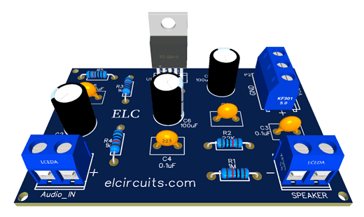
Fig. 1 - Layout of the Printed Circuit board

56W RMS Hi-FI Amplifier using LM3875 Integrated Circuit + PCB

For Portuguese version, click here! 

High-performance Hi-FI Audio Amplifier, capable of producing excellent audio quality, using the LM3875 integrated circuit.

The LM3875 is a high-performance power audio amplifier capable of delivering 56W of continuous power at load with 0.1% THD + N from 20Hz to 20KHz.

The LM3875 features an instantaneous temperature protection circuit with auto peak (° Ke) (SPiKe), which puts it in a class above discrete and hybrid amplifiers, inherently providing a safe operating area (SOA) dynamically protected by the circuits.

SPiKe protection, this means that the entire circuit is completely protected at the output against over-voltage, under-voltage, overloads caused by shorted outputs, thermal leaks, and instantaneous temperature spikes.

You might also be interested in:

The LM3875 maintains an excellent signal-to-noise transient rate above 95dB (min), with a typical low noise level of 2.0μV. It displays extremely low THD + N values ​​of 0.06% at the rated output into the rated and provides excellent linearity with a typical IMD (SMPTE) rating of 0.004%.

Features of LM3875

  • 56W continuous average output power at 8Ω
  • 100W instantaneous peak output capacity
  • Signal-to-noise ratio> 95dB (min)
  • Short-circuit protection to the ground or, to supplies via internal current limiting circuit
  • Output overvoltage protection against inductive load transients
  • Provides protection against under-voltage, not allowing internal polarization when | V + | + | V− | ≤ 12V, thus eliminating the activation transients are deactivated
  • 11 Lead PFM Package
  • Wide supply voltage range: | V + | + | V− | = 20V to 84V
  • Total harmonic distortion (THD) less than 0.03% in the frequency range of 20Hz to 20kHz

Power Supply Circuit

The power supply provided by a transformer AC,  which can be elaborated through a 28-0-28Vac,  with 5 Ampers current, which after going through the rectification, will be delivered in the supply range around +/- 40Vdc.

As we saw in the characteristics of the LM3875 above, it has a wide range of supply voltage, which we can use a lower voltage or higher voltage source, we can do with what we have on our bench.

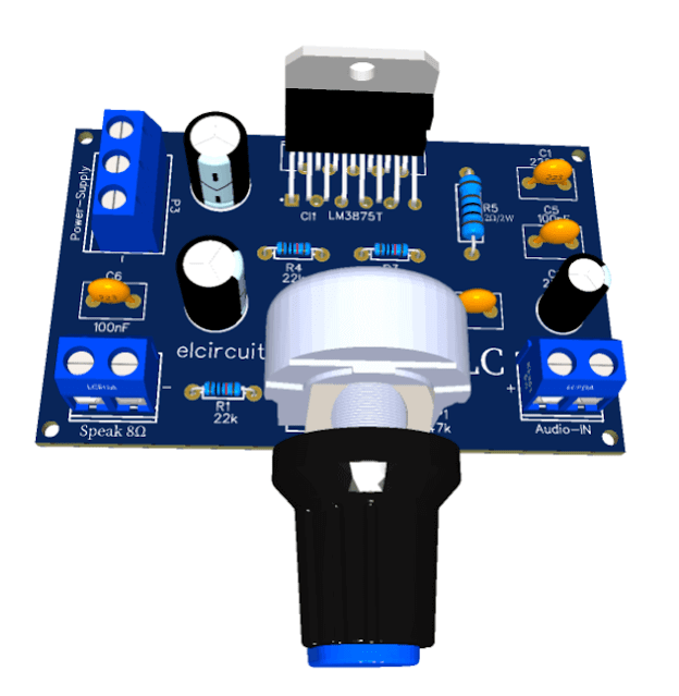
In Figure 2 below, we have the schematic diagram of the 56W Hi-End Amplifier with the LM3875 CI.

Fig. 2 - Schematic diagram of 56W RMS Hi-End Amplifier with LM3875 IC

Component List

  • CI 1 ----------------- Integrated Circuit LM3875T
  • R1, R4 -------------- Resistor 1 / 8w 22K
  • R2, R3 -------------- Resistor 1 / 8w 1K
  • R5 ------------------- Resistor 2w 2Ω
  • C1 ------------------- 220pF ceramic/polyester capacitor
  • C2 ------------------- Electrolytic Capacitor 22uF
  • C3, C4 -------------- 470uF Electrolytic Capacitor
  • C5, C6, C7 --------- 100nF ceramic / polyester capacitor
  • P1 ------------------- Potentiometer 47K
  • Others -------------- Wires, Welds, PCB, Etc.

Printed Circuit Board

The layout of the Printed Circuit Board is shown in Figure 1, and we have all the necessary files for you to be able to print your PCI, with the GERBER files, PDF Layout, PNG, all with a direct link for you to download and assemble yours.

Downloadable files

Files: Gerber, Layout in PDF, PNG, for download. Direct link: Click Here

I hope you enjoyed it!!!

If you have any questions, suggestions or corrections, please leave them in the comments and we will answer them soon.

Subscribe to our blog!!! Click here - elcircuits.com!!!

My Best Regards!!!

Saturday, October 10, 2020

HI-FI 30W Audio Power Amplifier using LM1875 IC + PCB

Figure 1 - PCB Hi-Fi 30W Power Amplifier LM1875

The amplifier presented, is a hi-fi amplifier based on the Integrated Circuit LM1875, which is a monolithic power amplifier offering very low distortion and high-quality performance for consumer audio applications.

General Description

The LM1875 delivers 20 watts into a 4Ω or 8Ω load on ±25V supplies. Using an 8Ω load and ±30V supplies, over 30 watts of power may be delivered.

The LM1875 is a wide power amplifier with very low distortion and high-quality efficiency for audio applications, the amplifier is designed to operate with a minimum of external components.

Device overload protection consists of both internal current limit and thermal shutdown.

You might also be interested in:

The LM1875 design takes advantage of advanced circuit techniques and processing to achieve extremely low distortion levels even at high output power levels.

Other outstanding features include high gain, fast slew rate, and wide power bandwidth, large output voltage swing, high current capability, and a very wide supply range. The amplifier is internally compensated and stable for gains of 10 or greater.

Features

  • Up to 30 Watts Output Power
  • AVO Typically 90 dB
  • Low Distortion: 0.015%, 1 kHz, 20 W
  • Wide Power Bandwidth: 70 kHz
  • Protection for AC and DC Short Circuits to Ground
  • Thermal Protection with Parole Circuit
  • High Current Capability: 4A
  • Wide Supply Range 16V-60V
  • Internal Output Protection Diodes
  • 94 dB Ripple Rejection
  • Plastic Power Package TO-220

Applications

  • High-Performance Audio Systems
  • Bridge Amplifiers
  •  Stereo Phonographs
  • Servo Amplifiers
  • Instrument Systems

The connection diagram or if you prefer, the pinout of the LM1875 is shown in Figure 2 below.

Figure 2 - Pinout LM1875 Audio Amplifier
 
The circuit diagram is in Figure 3 below, as we can see, there are few numbers of external components, making the assembly of this amplifier very easy.
Figure 3 - Schematic Audio Power Amplifier IC LM1875

Power Dissipation and Heat Sink

The LM1875 must always be operated with a heat sink, even when it is not required to drive a load. Assumes the use of a heat sink having a thermal resistance of 1°C/W and no insulator with an ambient temperature of 25°C. 

Because the output limiting circuitry has a negative temperature coefficient, the maximum output power delivered to a 4Ω load may be slightly reduced when the tab temperature exceeds 55°C.

Component List

  • U1 ......... LM1875 Integrated Circuit.
  • R1 ......... 1MΩ 1/8w Resistor (brown, black, yellow, gold)
  • R2 ......... 22KΩ 1/8w Resistor (red, red, orange, gold)
  • R3 ......... 1KΩ 1/8w Resistor (brown, black, red, gold)
  • R4 ......... 20KΩ 1/8w Resistor (red, black, orange, gold)
  • R5 ........  1Ω 1/8w Resistor (brown, black,  gold)
  • C1 ......... 2.2µF Polyester capacitor
  • C2 .....… 25V  22µF Electrolytic capacitor
  • C3, C4 ... 0.1uF Ceramic capacitor
  • C5 .......... 0.22uF Ceramic capacitor
  • C6, C7 ... 70V  100µF Electrolytic capacitor
  • P1, P3 .... Screw Terminal Block: 2-Pin, 5 mm
  • P2 .......... Screw Terminal Block: 3-Pin, 5 mm
  • Others .... printed circuit board, heat sink, box, tin, wires, etc.

Printed Circuit Board

The layout of the Printed Circuit Board is shown in Figure 1, and we have all the necessary files for you to be able to print your PCI, with the GERBER files, PDF Layout, JPG. All with a direct link for you to download and assemble yours.

Downloadable files

Files: Gerber, Layout in PDF, PNG, to download. Direct link: Click Here!

If you have any questions, suggestions or corrections, please leave them in the comments and we will answer them soon.

Subscribe to our blog!!! Click here - elcircuits.com!!!

My Best Regards!!!

Thursday, September 24, 2020

HI FI 32W Audio Amplifier - TDA2050 - Simple PS + PCB

Fig 1 - Hi-Fi 32W Audio Amplifier PCB

The circuit given here is a 32 Watt amplifier using the famous TDA2050V IC from ST Microelectronics.

The amplifier is built around a single integrated circuit, the TDA2050V that is an integrated monolithic 32 Watt class AB audio amplifier IC available in the Pentawatt package. The IC has a lot of good features as shown below.

  • High Output Power
  • 50W Music Power IEC 268.3 Rules
  • High Operating Supply Voltage - 50V
  • Single or Split Supply Operations
  • Very Low Distortion
  • Short Circuit Protection  - OUT to GND
  • Thermal Shutdown

Description

The TDA 2050 is a monolithic integrated circuit intended for use as an audio class AB audio amplifier. Thanks to its high power capability the TDA2050 is able to provide up to 35W true RMS power how showed below:

  • Into 4 ohm load @ THD = 10%, VS = ±18V, f = 1KHz up to 35W
  • Into 8 ohm load @ THD = 10%, VS = ±22V, f = 1KHz up to 32W
  • Into 4 ohm load over 1 sec at VS= 22.5V, f = 1KHz up to 50W

The high power and very low harmonic and crossover distortion THD = 0.05% typ, @ VS = ±22V, PO = 0.1 to 15W, RL=8ohm, f = 100Hz to 15KHz) make the device most suitable for both HiFi and high class TV sets.

The schematic diagram is shown in Figure 2 below, it is a simple circuit to assemble, and to use it in Stereo, we can assemble two of the same, one for each channel.

Fig. 2 - Schematic diagram Hi Fi 32W Audio Amplifier - TDA2050

Components List

The recommended values of the external components are those shown below. Different values can be used, however, to better performance, you must use these values.

Parts List

  • U1 ............................ Integrated Circuit TDA2050 Audio Power Amplifier
  • R1, R2, R3, R5 ........ 22KΩ 1/4w Resistor
  • R4 ............................ 680Ω 1/4w Resistor
  • R6 ............................ 2.2Ω 1/4w Resistor
  • C1 ............................ 2.2uF /25V Electrolytic capacitor
  • C2 ............................ 100uF /25V Electrolytic capacitor
  • C3, C7 ..................... 1000uF /50V Electrolytic capacitor
  • C4 ............................ 22uF /25V Electrolytic capacitor
  • C5 ............................ 100nF  Polyester Capacitor
  • C6 ............................. 0.47uF Polyester Capacitor
  • RP1 .......................... 47KΩ Potentiometer
  • P1, P2, P3 ................ Screw Terminal Block: 2-Pin, 5 mm
  • Miscellaneous .......... Heatsink, screw, solder, etc.

Printed Circuit Board

We're providing the Printed Circuit Board, we leave the GERBER, PDF, LAYOUT files, to be downloaded at the link below.

Downloadable files

Files: Gerber, Layout in PDF, PNG, for download. Direct link: Click Here!

If you have any questions, suggestions or corrections, please leave them in the comments and we will answer them soon.

Subscribe to our blog!!! Click here - elcircuits.com!!!

My Best Regards!!!

Monday, September 14, 2020

How Switched Mode Power Supply Works - SMPS - ATX

ATX Switched-Mode Power Supplies have some interesting features when compared to standard Switched Mode Power Supply (SMPS).

In the ATX power supply, there are different output voltages: + 12V, + 5V, + 3.3V, -12V, -5V and 5VSB. There are some variations on these types of Power Supply, but in the general context, the pattern is this.
The way SMPS work is pretty much the same.
They control the output voltage by opening and closing the switching circuit so as to maintain the opening and closing time of this circuit, that is, the width of the pulses and their frequencies, to obtain the desired voltage.

There are separate processes for everything to work smoothly.
So let's see the modular diagram to unravel the steps of these processes so that we can step by step understanding.
This is the block in modules divided by steps, to improve our understanding.
 
 
There are 10 basic steps to running an ATX power supply, there are other underlying modules that are intrinsic in the steps, but, we'll not go as deep as it would be extremely great this Blogger, for those who want to watch the explanatory video with details in Portuguese. On the original post channel from YouTube.

Original Portuguese Version: Click Here

Step 1 - Transient Filter

Is through that stage that the voltage coming from your network, whether 110 or 220V AC should enter.
Transient Filter

This voltage goes through basic protection, the fuse, that if some step ahead short, the fuse opens, avoiding to burst everything ahead, and in the same line, we have the NTC (Negative Temperature Coefficient), It's a surge current limiter, in series with the electric circuit,

In it the value of ohmic resistance decreases as its temperature rises, its initial resistance is approximately 15 Ohms, which we can understand by the Ohms' law, the advantages one has in using it in series after the power supply switches it on lowers its resistance to approximately 0.5 Ohms.

EMI filters also exist, these are used to avoid high-frequency noise and a huge amount of harmonics generated by the switches that can propagate through the electrical network and cause interference in nearby electronic equipment.

Step 2 - Primary Rectification

Primary Rectification
 
In this stage we find the rectifier bridge or an arrangement formed by four common diodes, which has the function of rectifying a full-wave voltage, that is, rectifying an alternating electric current (AC), transforming it into a continuous electric current ( DC).

Step 3 - Filtration

Filtration
 
After rectification, the DC signal, Ripples (which are small variations, the capacitors are responsible for the filtering and stabilization IE, a decrease of these Ripples, in the rectified voltage, this voltage rises to something around 300V, which are used in the power switches, this part is fundamental to the correct stabilization of the source especially if its source is of high power.

Step 4 - Power Switches

Power Switches
 
These switches can be Bipolar Power Transistors such as MOSFETs, or any other type, but they differ from ordinary transistors, by the type of operation in which these transistors work, these switching transistors dissipate less power than a common working transistor in a linear source because they work as a switch on / off at high speeds, depending on the design of the source, they suffer variations that are usually between 20Khz to 100kHz, they are directly responsible for the output voltage, and stability of that voltage, through of the commands received by the Control Circuit.

Step 5 - Output Transformer

Output Transformer
 
The transformer is a high-frequency CHOPPER TRANSFORMER, and they also work with alternating voltage, when passing through the switches the voltage will be a square wave AC type PWM, but with high frequency, not with the same frequency of 60Hz of the input voltage.

The switches work on two different levels, High and Low, when it is HIGH, the voltage goes through it normally, causing a constant voltage level in the input of the coil of the transformer, the action of these transistors, goes from HIGH to LOW very quickly.

This will induce the winding to have the necessary voltages according to the winding and frequency placed on these switches.

Step 6 - Fast Rectifier

Fast Rectifier

With the voltage generated by high-frequency switches, a diode is needed to meet this demand, so we have the high-speed diodes called SCHOTTKY DIODES or fast recovery diodes since ordinary diodes would not be able to work with high-frequency voltages.

Step 7 - Output Filters

Output Filters

The inductor - This has the function of eliminating the high-frequency harmonics so that they do not travel to the equipment that will be fed, imagine if these harmonics pass to a micro-controller for example, could cause undue loads and errors of reading in the control processes.

And the Capacitors - They are the ones that filter and stabilize the voltage at the output, avoiding ripples and instabilities at the output.

Step 8 - Driver Transformer

Driver Transformer
 
The driver transformer in this case is nothing less than the one responsible for traffic the information coming from the Integrated Circuit Controller, and pass these commands to the switches, so as to bring insulation or electrical decoupling between primary and secondary, in this topology there is a pair of transistors that also switch the Transformer Drive to receive these PWM pulses from the driver IC, passing this information to the power step we already saw in Step 4.

Step 9 - PWM control

PWM control
 
The brain of a switched source is its PWM controller, they are dedicated integrated circuits, to perform that work, but they do not work alone, there are also current sensors, which also vary from source to source, but it is very likely that you will find in its source the TL341 IC, it has the aspect of a transistor, but, it is not a transistor, it is very popular for its cost-benefit.

This circuit is connected to the output of the power supply, receives Feedback, and directs the voltage information to the IC that controls the oscillator that generates a rectangular signal whose pulse width is controlled and sent to the Transformer Drive that sends these commands to the step of power.

If the power at the output to raise the voltage tends to drop, the circuit activates the instantaneous correction in the pulse width of the switching transistors and the voltage keeps stabilized.

Step 10 – Primary Power Supply VSB

Primary Power Supply VSB
 
VSB stands for Voltage Standby, which is technically a power supply that keeps its output active, whenever the source power cord is connected to the mains, its capacity is approximately 2 Amps, and this depends on the total power of the source, this active voltage line is to keep the circuit active and is necessary for when the power on button is activated through PSON, which is the start of the power supply, then the oscillator will activate the power line also powers the motherboard hardware to activate peripherals via software, keyboard, network, and so on.

If you have any questions, suggestions or corrections, please leave them in the comments and we will answer them soon.

Subscribe to our blog!!! Click here - elcircuits.com!!!

My Best Regards!!!

Sunday, September 13, 2020

5W BTL Audio Amplifier with DC volume control + PCB

Fig. 1 - 5W BTL Audio Amplifier PCB


This audio amplifier circuit is based on the TDA7056B, that's a mono Bridge-Tied Load (BTL) output amplifier with DC volume control. It is designed for use in, PC audio amplifiers, TVs, and monitors, but is also suitable for battery-fed portable recorders and radios. The device is contained in a 9-pin medium power package.

A Missing Current Limiter (MCL) is built-in. The MCL circuit is activated when the difference in current between the output terminal of each amplifier exceeds 100 mA (300 mA Typ.). This level of 100 mA allows for headphone applications (single-ended).

You might also be interested in:

This TDA7056 audio amplifier will provide a maximum output power of 5 watts into an 8 ohms load using a 6 volts power supply, or maximum output power of 3 watts into a 16 ohms load using an 11 volts power supply.

Fig. 2 - Schematic TDA7056 Audio Amplifier

The audio gain of the  IC is internally fixed at 40 dB. The maximum input voltage supported by this circuit is 18 volts. As we can see in the Figure 2  circuit diagram, we will need only a few components to build this audio amplifier.

VOLUME CONTROL

In conventional DC volume circuits, the control or input stage is coupled to the output stage via external capacitors to keep the compensation voltage low. In the TDA7056B, the DC volume control stage is integrated with the input stage, so coupling capacitors are not required. 

With this configuration, a low compensating voltage is still maintained and the minimum supply voltage remains low.

FEATURES

  • DC volume control
  • Few external components
  • Mute mode
  • Thermal protection
  • Short-circuit proof
  • No switch-on and switch-off clicks
  • Good overall stability
  • Low power consumption
  • Low HF radiation
  • ESD protected on all pins.

Material list

  • U1........................... TDA7056 – Audio Amplifier Integrated circuit
  • C1 .......................... 1uF - 25V – Electrolytic capacitor
  • C2 .......................... 0.47uF – Polyester Capacitor
  • C3 .......................... 100uF - 25V – Electrolytic capacitor
  • R1 .......................... 100K ohms - 1/8 W – "brown, black, yellow, gold"
  • R2 .......................... 1K ohms - 1/8 W – "brown, black, red, gold"
  • RP1 ........................ 22 k ohms –  Potentiometer
  • P1, P2, P3 ............... Kre Block Terminal Terminal 2-Way Double Connector
  • Miscellaneous ........ Printed Circuit Board, tin, wire, etc.

We are offering to download the link with the printed circuit board printing files, they are; Gerber, PDF layout, PNG, all the files with a direct link to Mega.

Direct link to download

Click in the link  to download the Files: PCB Layout, PDF, GERBER

If you have any questions, suggestions or corrections, please leave them in the comments and we will answer them soon.

Subscribe to our blog!!! Click here - elcircuits.com!!!

My Best Regards!!!

Saturday, September 12, 2020

PinOut - ARDUINO UNO Board - ATMega328PU

Main Features

Arduino UNO is a microcontroller board based on the ATmega328P. It has 14 digital input/output pins (of which 6 can be used as PWM outputs), 6 analog inputs, a 16 MHz ceramic resonator, a USB connection, a power jack, an ICSP header and a reset button. 

It contains everything needed to support the microcontroller; simply connect it to a computer with a USB cable or power it with a AC-to-DC adapter or battery to get started. 

You can tinker with your UNO without worrying too much about doing somethin

Click here to Datasheet

Source: arduino.cc

If you have any questions, suggestions or corrections, please leave them in the comments and we will answer them soon.

Subscribe to our blog!!! Click here - elcircuits.com!!!

My Best Regards!!!