Wednesday, December 8, 2021

24W Stereo Hi-Fi Audio Amplifier using TDA2616 + PCB

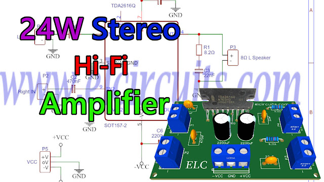
Fig.- 24W Stereo Hi-Fi Audio Amplifier using TDA2616 + PCB

In this article, we show you how to build a simple and portable 12W + 12W audio amplifier using the TDA2616 Integrated Circuit.

The TDA2616 IC is a stereo power audio amplifier, it comes with plastic package (SOT131) single-in-line 9-lead (SIL9).

This IC is explicitly designed for mains powered amplifier circuits, such as stereo radio, instrument return box, TV sets and so on.

The TDA2616 IC has a good input gain balance on both channels in accordance with IEC 268 and DIN 45500 standards.

In addition, the TDA2616 has a special integrated circuit for the suppression of noise signals at the inputs during activation and deactivation, which avoids clicking sounds or the famous popping during circuit operation.

You might also be interested in:

Features

  • Requires very few external components
  • No switch-on/switch-off clicks
  • Input mute during switch-on and switch-off
  • Low offset voltage between output and ground
  • Excellent gain balance of both amplifiers
  • Hi-fi in accordance with IEC 268 and DIN 45500
  • Short-circuit proof and thermal protected
  • Mute possibility.

In Figure 2 below, we show the complete 24W Stereo Audio Amplifier Circuit using TDA2616 IC, as we can see, there are few external components, which makes it easier for those who do not have much experience with assembling electronic circuits.

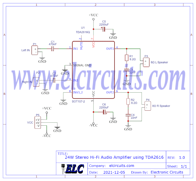
Fig. 2 - Schematic 24W Stereo Hi-Fi Audio Amplifier with Mute using TDA2616

Amplifier Operation 

This amplifier circuit was designed to work with a symmetrical power supply, the maximum power supply voltage is 21V, however the recommended is 16V, with this voltage, an output power of 2 × 12 W is obtained (with THD = 0 .5%) with a load of .

The mute circuit can also be activated via pin 2. When a current of 300µA is present at pin 2, the circuit is in the mute condition.

The internal gain voltage is fixed at 30dB, which allows us a stable balance between the two amplifier channels (0.2dB).

Components List

  • U1 ....................... TDA2616 Integrated circuit

  • R1, R2 ................ 8.2Ω resistor (brown, black, orange, gold)

  • C1, C2 ................ 470nF ceramic, polyester capacitor 
  • C3, C4 ................ 22nF ceramic, polyester capacitor 
  • C5, C6 ................ 2200uF / 25V electrolytic capacitor

  • P1, P2, P3, P4 .... Screw Terminal Type 5mm 2-Pin Connector
  • P5 ....................... Screw Terminal Type 5mm 3-Pin Connector
    • Others ................ PCB, tin, wires, soldering Iron, etc.

    Download

    We provide the files with the PCB, the schematic, the PDF, GERBER and JPG, PNG and provide a direct link for free download and a direct link, "MEGA".

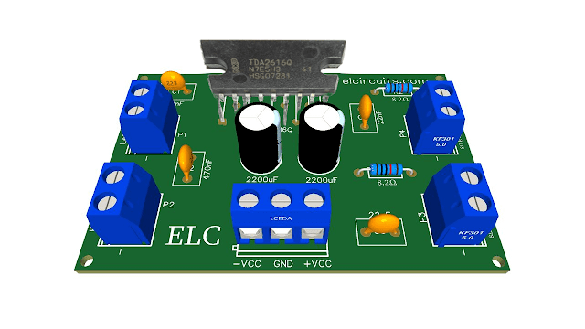
    Fig. 3 - PCB - 3D - 24W Stereo Hi-Fi Audio Amplifier with Mute using TDA2616

    Click on the direct link to download the files: Layout PCB, PDF, GERBER, JPG

    If you have any questions, suggestions or corrections, please leave them in the comments and we will answer them soon.

    Subscribe to our blog!!! Click here - elcircuits.com!!!

    My Best Regards!!!


    Monday, December 6, 2021

    Adjustable Switching Power Supply 5.1 to 40V, 2.5 Amp using L4960 + PCB

    Fig. 1 - Adjustable Switching Power Supply 5.1 to 40V, 2.5 Amp using L4960

    In this article, we present an adjustable power supply with a stabilized output that varies from 5.1 to 40V, with a current of 2.5 amps

    This one can also have its stabilized voltage fixed, everything will depend on the type of project you are going to use.

    The adjustable power supply is based on IC L4960 which is a monolithic power switching regulator IC, delivering 2.5A at a voltage variable from 5V to 40V in step down configuration.

    Features of the device include current limiting, soft start, thermal protection and 0 to 100% duty cycle for continuous operation mode.

    The complete schematic diagram of the power supply is shown below in Figure 2, it is a simple but complete power supply.

    Fig. 2 - Schematic Adjustable Switching Power Supply 5.1 to 40V, 2.5 Amp using L4960

    CIRCUIT OPERATION

    The L4960 is a monolithic step down switching regulator providing output voltages from 5.1V to 40V and delivering 2.5A.

    The regulation loop consists of a sawtooth oscillator, error amplifier, comparator and the output stage. An error signal is produced by comparing the output voltage with a precise 5.1V on-chip reference (zener zap trimmed to ± 2%).

    This error signal is then compared with the sawtooth signal to generate the fixed frequency pulse width modulated pulses which drive the output stage.

    The gain and frequency stability of the loop can be adjusted by an external RC network connected to pin 3. 

    Closing the loop directly gives an output voltage of 5.1V. Higher voltages are obtained by inserting a voltage divider.

    You may be interested in: 

    Output overcurrent at switch on are prevented by the soft start function. The error amplifier output is initially clamped by the external capacitor Css and allowed to rise, linearly, as this capacitor is charged by a constant current source. Output overload protection is provided in the form of a current limiter.

    The load current is sensed by an internal metal resistor connected to a comparator. When the load current exceeds a preset threshold this comparator sets a flip flop which disables the output stage and discharges the soft start capacitor. 

    A second comparator resets the flip flop when the voltage across the soft start capacitor has fallen to 0.4V.

    The output stage is thus re-enabled and the output voltage rises under control of the soft start network.

    If the overload condition is still present the limiter will trigger again when the threshold current is reached. The average short circuit current is limited to a safe value by the dead time introduced by the soft start network. 

    The thermal overload circuit disables circuit operation when the junction temperature reaches about 150°C and has hysteresis to prevent unstable conditions.

    Efficient operation at switching frequencies up to 150KHz allows a reduction in the size and cost of external filter components.

    The L4960 is mounted in a plastic Heptawatt power pack, and the pinouts are shown in Figure 3 below.

    Fig. 3 -  L4960 IC Heptawatt Pinout

    Download

    We provide the files with the PCB, the schematic, the PDF, GERBER and JPG, PNG and provide a direct link for free download and a direct link, "MEGA".

    Click on the direct link to download the files: Layout PCB, PDF, GERBER, JPG

    Fig. 4 - Adjustable Switching Power Supply 5.1 to 40V, 2.5 Amp using L4960

    If you have any questions, suggestions or corrections, please leave them in the comments and we will answer them soon.

    Subscribe to our blog!!! Click Here - elcircuits.com!!!

    My Best Regards!!!

    Friday, December 3, 2021

    5W Stereo Audio Amplifier Circuit using TEA2025 IC + PCB

    In this article, we show you how to build a simple and portable 5W stereo audio amplifier using the TEA 2025 Integrated Circuit.

    This circuit built based on TEA2025 IC which is a monolithic integrated audio amplifier in a 16-pin plastic dual in line package manufactured by UTC

    The circuit has Internal Thermal Protector. It is designed for portable cassette players, mp3 players and radios. 

    You can also use it as your smartphone or PC audio amplifier. This circuit requires 9V power supply to work, you may use a power supply circuit with output 9V 500mA DC current or a 9V lead acid battery.

    Features

    • The power supply voltage range is from 3V to 15V.
    • Working Voltage down to 3V
    • Few External components
    • Dual or Bridge Connection Modes
    • High Channel isolation
    • Very low switch On/Off Noise
    • Voltage gain up to 45dB(Adjustable with external resistor)
    • Soft clipping
    • Internal Thermal protection

    Working Explanation

    This amplifier, in the configuration presented in this article, is 2 channels, has an output power of 2.5 watts per channel.

    For those who want to use a single channel, you can be using it in bridge mode, and you will have an output power of 5W.

    Input Capacitor

    The input capacitor is PNP type, allowing the source to be referenced to ground. In this way, no input coupling capacitor is required. 

    However, a series capacitor (0.22 uF)to the input side can be useful in case of noise due to variable resistor contact.

    Bootstrap

    The bootstrap connection allows increasing the output swing. The suggested value for the bootstrap capacitors (100uF) avoids a reduction of the output signal also at low frequencies and low supply voltages.

    This amplifier in this 2-channel configuration, has an output power of 2.5 watts per channel, and you may be using it in bridge mode, and you will have an output of 5W.

    Power supply

    The power supply is direct current, "Vdc", the voltage supported by this amplifier is up to 15V, with a peak current of 1.5 amps.

    The voltage input pin is located on pin 16 of  TEA2025 IC, while pins 4, 5, 9, 13, 12 are grounded to GND.

    Applications

    • Electronic Instruments
    • PC sound speaker
    • Home theater systems
    • Hi-fi electronic gadgets and devices
    • Robotics applications 
    • Children’s gadgets and toys, etc.

    In Figure 1 below, we show the complete 5W Stereo Audio Amplifier Circuit using TEA2025 IC, and that you can download the files in option; Download files below at the bottom of the page.

    Fig. 1 - Schematic 5W Stereo Audio Amplifier Circuit using TEA2025 IC

    Components List

    • U1 ................................ TEA2025 Integrated circuit

    • R1, R2 ......................... 10K resistor (brown, black, orange, gold)

    • C1, C2 ......................... 0.47uF ceramic, polyester capacitor 
    • C3, C4, C5, C6, C9 ..... 100uF electrolytic capacitor
    • C7, C11 ....................... 470uF electrolytic capacitor
    • C8, C10 ....................... 0.15uF ceramic, polyester capacitor 

    • P1, P2, P3, P4, P5 ....... Screw Terminal Type 5mm 2-Pin Connector
    • Others ......................... PCB, tin, wires, etc.

    PCB - Download

    We provide the files with the PCB, the schematic, the PDF, GERBER and JPG, PNG and provide a direct link for free download and a direct link, "MEGA".

    Fig. 2 - 5W Stereo Audio Amplifier Circuit using TEA2025

    Click on the direct link to download the files: Layout PCB, PDF, GERBER, JPG

    If you have any questions, suggestions or corrections, please leave them in the comments, and we will answer them soon.

    Subscribe to our blog!!! Click here - elcircuits.com!!!

    My Best Regards!!!

    Thursday, December 2, 2021

    High Precision 5 Volts 3 Amp Voltage Regulator Circuit using TL431 + PCB

    Circuits with a high level of sensitivity require a stable supply, they are generally difficult to be powered by power supplies, due to the high level of sensitivity needed to provide stable voltage in the circuit.

    However, we are introducing a stabilized power supply with an accurate output to power any sensitive circuit, such as microcontroller circuits, microprocessor circuits, RF transmission, PICs, and so on.

    Today we are going to build a very precise circuit, which uses a very well-known component that is widely used in SMPS power supplies, especially ATX PC power supplies, “which looks more like a transistor”.

    The 3-Pin TL431 Integrated Circuit, It offers better stability, less temperature deviation (VI (dev)) and less reference current (Iref) for greater system accuracy.

    You may be interested in: 

    The TL431 device is an adjustable tap regulator with thermal stability specified in the applicable automotive, commercial, and military temperature ranges.

    The output voltage can be set to any value between Vref (approximately 2.5V) to 36V, with two external resistors. These devices have a typical output impedance of 0.2 Ω.

    The active output circuitry provides a very crisp activation characteristic, making these devices excellent replacements for Zener diodes in many applications such as integrated regulation, tunable power supplies and switched power supplies.

    Characteristics

    • Reference voltage tolerance at 25°C
    • 0.5% (class B)
    • 1% (class A)
    • 2% (standard class)
    • Adjustable output voltage: Vref to 36V
    • Operation from -40 °C to 125 °C
    • Typical temperature deviation (TL43xB)
    • 6 mV (temperature C)
    • 14 mV (I Temp, Q Temp)
    • Low output noise
    • 0.2 Ω typical output impedance
    • Sink current capacity: 1 mA to 100 mA
    • Application
    • Adjustable voltage and current reference
    • Secondary lateral adjustment in Flyback SMPSs
    • Zener Replacement
    • voltage monitoring
    • Comparator with integrated reference

    In Figure 2 below, we have the schematic diagram of the High Precision Voltage Regulator Circuit with TL431 IC, the LM350 IC, provides a current of up to 3 Amps.

    Fig. 1 - High Precision 5 Volts 3 Amp Voltage Regulator Circuit - TL431

    With the TL431 IC, they provide a precise 5V output, which is often necessary for precision microcontrollers, sensitive equipment, that require a stabilized voltage, this circuit is ideal for that.

    The power supply must provide a current of at least 3 Amps. Its input voltage must be greater than 7 Volts, to avoid overheating the LM350 IC, voltages no greater than 15V must be used.

    Components List

    • CI 1 ......... Voltage Regulator Circuit LM350
    • CI 2 ......... Adjustable Regulator Circuit TL431
    • R1 ........... 8K2Ω Resistor (grey, red, red)
    • R2, R3 ..... Precision resistor 243Ω 1% (red, yellow, orange, black, brown)
    • P1, P2 ..... Soldering terminals on 2-pin PCI
    • Others ..... Printed Circuit Board, tin, wires, etc.

    Download

    We provide the files with the PCB, the schematic, the PDF, GERBER and JPG, PNG and provide a direct link for free download and a direct link, "MEGA".

    Fig. 2 - High Precision 5 Volts 3 Amp Voltage Regulator Circuit - TL431

    Click on the direct link to download the files: Layout PCB, PDF, GERBER, JPG

    If you have any questions, suggestions or corrections, please leave them in the comments and we will answer them soon.

    Subscribe to our blog!!! Click here - elcircuits.com!!!

    My Best Regards!!!

    Monday, November 29, 2021

    Symmetrical Power Supply for Power Amplifiers using Calculation + PCB

    Fig. 1 - Symmetrical Power Supply for Power Amplifiers

    For power amplifier lovers, who build their own audio power amplifiers, here is a good full wave rectifier linear symmetric power supply that will meet the power demand without leaving anything to be desired in terms of stability.

    This power supply is designed for amplifiers with power up to 2500W, it will work without any problems with great stability.

    Most power amplifier circuits require a symmetrical power supply, and what differs from each other is always the power required from the supply.

    As we know, a good power supply with good filtering will determine the quality and final power of your amplifier.

    You may be interested in: 

    The complete schematic diagram of the power supply is shown below in Figure 2, it is a simple but complete power supply.

    Fig.2 - Electrical schematic Symmetrical Power Supply for Power Amplifiers


    However, it is worth remembering that for each amplifier power range, we can assemble a type of power supply according to the power of your amplifier.

    We are presenting 3 different configurations to exemplify the different types of power amplifiers.

    There are 3 examples of simplified formulas for you to calculate the  power supply Current and Voltage according to the power of your amplifier.

    Remembering that the PCB printed circuit board is the same for all configurations.

    Configuration 1:

    In this configuration, we can use amplifiers that have a total power up to 400W

    We need to calculate the maximum power supply current, considering 45V supply, and the maximum power of 400W. Calculating ohms Law: P = V * I
    • I = P / V 
    • I = 400/45 
    • I = 8.88A
    Now you need to stipulate the maximum ripple allowed in your design, in this case: If you set the maximum ripple voltage to 5%!
    • V_ripple = V_ps * 5%
    • V_ripple = 45V * 5%
    • V_ripple  = 2.25V
    Once the maximum ripple voltage has been stipulated, we need to calculate the capacitor for that ripple at 5% of the source, "You may be calculating the percentage that best suits your design."

    Capacitor Calculation Formula : C = I / F * V_ripple 
    • C = 8.88 / 120 * 2.25
    • C = 8.88 / 270
    • C = 0.032888 = > C = 32.888X10^-6 = 32.888uF
    As our board was designed to support 6 capacitors. We can divide the entire value into uF and divide by 6 Capacitors.
    • C_individual = 32.888 / 6
    • C_individual  = 5.481uF

    For a closer commercial capacitors value, we have:
    C_individual = 6.800uF / 63V

    • 6 x 6.800uF Capacitor
    • 15A rectifier bridge

    Configuration 2:

    In this configuration, we can use amplifiers that have a total power up to 1200W

    We need to calculate the maximum power supply current, considering 75V supply, and the  maximum power of 1200W. Calculating ohms Law: P = V * I
    • I = P / V 
    • I = 1200/75 
    • I = 16A

    Now you need to stipulate the maximum ripple allowed in your design, in this case: If you set the maximum ripple voltage to 5%!
    • V_ripple = V_ps * 5%
    • V_ripple = 75V * 5%
    • V_ripple  = 3.75V

    Once the maximum ripple voltage has been stipulated, we need to calculate the capacitor for that ripple at 5% of the source, "You may be calculating the percentage that best suits your design."

    Capacitor Calculation Formula : V_ripple = I / F * C
    • C = I / F * V_ripple 
    • C = 16 / 120 * 3.75
    • C = 16 / 450
    • C = 0.035555 = > C = 35.555X10^-6 = 35.555uF

    As our board was designed to support 6 capacitors. We can divide the entire value into uF and divide by 6 Capacitors.
    • C_individual = 35.555 / 6
    • C_individual  = 5.925uF

    For a closer commercial capacitors value, we have:
    C_individual = 6.800uF / 100V

    • 6 x 6.800uF Capacitor
    • 25A rectifier bridge

    Configuration 3:

    In this configuration, we can use amplifiers that have a total power up to 2500W

    We need to calculate the maximum power supply current, considering 95V supply, and the maximum power of 2500W. Calculating ohms Law: P = V * I
    • I = P / V 
    • I = 2500/95 
    • I = 26A

    Now you need to stipulate the maximum ripple allowed in your design, in this case: If you set the maximum ripple voltage to 5%!
    • V_ripple = V_ps * 5%
    • V_ripple = 95V * 5%
    • V_ripple  = 4.75V

    Once the maximum ripple voltage has been stipulated, we need to calculate the capacitor for that ripple at 5% of the source, "You may be calculating the percentage that best suits your design."

    Capacitor Calculation Formula : C = I / F * V_ripple 
    • C = 26 / 120 * 4.75
    • C = 26 / 570
    • C = 0.045614 = > C = 45.614X10^-6 = 45.614uF
    As our board was designed to support 6 capacitors. We can divide the entire value into uF and divide by 6 Capacitors.
    • C_individual = 45.614 / 6
    • C_individual  = 7.602uF

    For a closer commercial capacitors value, we have:
    C_individual = 10.000uF / 200V

    • 6 x 10.000uF Capacitor
    • 40A rectifier bridge

    Download

    We provide the files with the PCB, the schematic, the PDF, GERBER and JPG, PNG and provide a direct link for free download and a direct link, "MEGA".

    Click on the direct link to download the files: Layout PCB, PDF, GERBER, JPG

    If you have any questions, suggestions or corrections, please leave them in the comments and we will answer them soon.

    Subscribe to our blog!!! Click here - elcircuits.com!!!

    My Best Regards!!!

    Wednesday, November 10, 2021

    3-Band Active Equalizer Circuit using LF353 IC + PCB

    Fig. 1 - PCB 3-Band Active Equalizer Circuit with LF353 IC


    This three-band active graphic equalizer circuit is an active filter set for three basic audio equalization ranges, bass, mid and treble. The circuit is based on the LF353 operational amplifier integrated circuit.

    The LF353 is a two-input JFET operational amplifier with an internally compensated input offset voltage. The JFET input device provides wide bandwidth, low input bias currents and offset currents.

    You might also be interested in:

    Features

    • Internally Trimmed Offset Voltage: 10 mV
    • Low Input Bias Current: 50pA
    • Low Input Noise Voltage: 25 nV/√Hz
    • Low Input Noise Current: 0.01 pA/√Hz
    • Wide gain bandwidth: 4 MHz
    • High slew rate: 13V / μs
    • Low Supply Current: 3.6 mA
    • High Input Impedance: 1012Ω
    • Low Total Harmonic Distortion : 0.02%
    • Low 1/f Noise Corner: 50 Hz
    • Fast Settling Time to 0.01%: 2 μs

    The equalizer circuit.

    The 3-band Equalizer use a Integrated Circuits operational amplifier LF353, and the capacitors determine the frequencies, the higher their capacitance, the lower the cutoff frequencies.

    The proposed equalizer is a 2-octave graphic equalizer with a 3-band circuit, the cut-off frequencies are at: 150Hz, 1kHz and 12kHz.

    This circuit was assembled with LF353, but nothing prevents you from using other replacement pin compatible ICs, such as: LM1558RC4558, LM358 etc.
     
    The recommended supply voltage is between ±11V and ±15V, but note that the maximum voltage IC supports is ±18V. The IC consumption current is 6.5mA maximum, and 3.6mA average.

    The IC has two internal amplifiers, we get a amplifier for each frequency and the last one for the final amplification of the entire circuit. In Figure 2 below, the pinout and configuration of the LF353 integrated circuit is shown.

    Fig. 2 - Pinout IC LF353

    In Figure 3 below, we show the complete 3-band equalizer circuit, and that you can download the files in option; Download files below at the bottom of the page.

    Fig. 3 - Schematic Diagram 3-band Active Equalizer Circuit with LF353 IC

    Components List

    • U1 .............. Integrated circuit LF353

    • R1, R2, R5, R6 ... 10K resistor (brown, black, orange, gold)
    • R3, R7 ................ 3.6K resistor (orange, green, red, gold)
    • R4, R8 ................ 1.8K resistor (brown, gray, red, gold)

    • C1 ...................... 4.7uF electrolytic capacitor
    • C2 ...................... 1uF electrolytic capacitor
    • C3 ...................... 50nF polyester capacitor 
    • C4, C6 ............... 5nF polyester capacitor
    • C5 ...................... 22nF polyester capacitor

    • VR1 .................... 47K Potentiometer 
    • VR2, VR3 .......... 100K Potentiometer 
    • VR4 .................... 500K Potentiometer 

    • P1  ....................... Screw Terminal Type 5mm 3-Pin Connector
    • P2, P3 .................. Screw Terminal Type 5mm 2-Pin Connector
    • Others .................. PCB, tin, wires, etc.

    Download

    We provide the files with the PCB, the schematic, the PDF, GERBER and JPG, PNG and provide a direct link for free download and a direct link, "MEGA".

    Click on the direct link to download the files: Layout PCB, PDF, GERBER, JPG

    If you have any questions, suggestions or corrections, please leave them in the comments and we will answer them soon.

    Subscribe to our blog!!! Click here - elcircuits.com!!!

    My Best Regards!!!