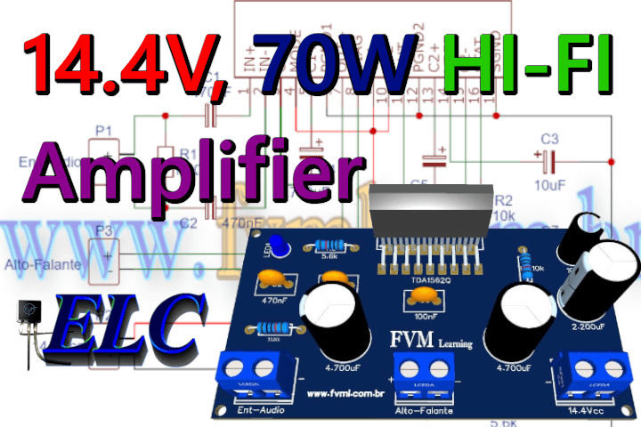
🌐 Idioma / Language: English English Português Português Español Español

Thursday, January 27, 2022

12 Volts Automatic Lead Acid Battery Charger Using LM350 IC with PCB

12 Volts Automatic Lead Acid Battery Charger Circuit + PCB

This is a 12V Automatic Lead Acid Battery Charger Circuit, of the type used in nobreaks, with loads ranging from 1A to 9 Amps.

The main advantage of this battery charger circuit is its charging mode, since it has a charge control, so that the battery does not receive voltage when it is not needed, giving more autonomy to the battery and protecting it from overvoltage.

What is Lead Acid Battery

The lead acid battery is a type of rechargeable battery first invented in 1859 by French physicist Gaston Planté

It is the first type of rechargeable battery ever created. Compared to modern rechargeable batteries, lead-acid batteries have relatively low energy density. 

Despite this, their ability to supply high surge currents means that the cells have a relatively large power-to-weight ratio. 

These features, along with their low cost, make them attractive for use in motor vehicles to provide the high current required by starter motors.

Lead Acid Battery Charger Method

There are several features related to the charging process of various battery segments and classes. 
The charging method for lead-acid batteries differs from NiCd batteries in the voltage limit, rather than the current limit to be used.

The charging time for lead-acid (sealed) batteries is 8 to 16 hours, depending on the capacity of the battery and the method used. 

With higher charging currents and multi-stage charging methods, the charging time can be reduced to 8 hours or less. 

For a multi-stage charger, three stages of charging application are required: 

  •  Constant current
  •  Peak charge
  •  Float charge

The Circuit

In Figure 2 below, we have the schematic diagram of the lead-acid battery charger circuit. It is a very simple circuit, with few external components, easy to assemble, yet even with its simplicity it works very well.

Schematic Circuit 12 Volts Automatic Lead Acid Battery Charger Circuit
Fig. 2 - Schematic Circuit 12 Volts Automatic Lead Acid Battery Charger Circuit

You may be interested in: 

How it Works?

The voltage regulation for charging the battery is done by the LM350 IC voltage regulator. The charging current control is done using the BC548B NPN transistor, it controls the demand current from the battery, causing the circuit to activate or deactivate the voltage required for charging the battery.

The potentiometer RP1 1K is used for fine tuning the battery charging voltage, which should be adjusted by using a multimeter to measure the output voltage, which should be at most 20% of the nominal battery voltage.

If you cannot find the description of the battery charging voltage on the battery itself, you can adjust the average charging voltage, which ranges from 13.8V to 14.4V.
It is necessary to use a heat sink in the voltage regulator, since the initial current to charge the battery is high. 

As the circuit charges the battery, it lowers the charging current until it reaches zero voltage, when the battery is fully charged.

Components List

  • Semiconductors
    • U1 .......... LM350 Voltage Regulator Circuit
    • Q1 .......... BC548B NPN Transistor
    • D1 .......... 1N5408 Silico Diode

  • Resistor
    • R1 .......... 100Ω Resistor (brown, black, brown, gold)
    • R2 .......... 0.5Ω 5W Resistor (green, black, silver, gold
    • R3 .......... 470Ω Resistor (yellow, violet, brown, gold)
    • R4 .......... 120Ω Resistor (brown, red, brown, gold)
    • RP1 ........ 1KΩ Potentiometer

  • Capacitor
    • C1 .......... 2.2uF / 25V Electrolytic Capacitor
    • C2 .......... 0.33uF / 25V Electrolytic Capacitor
       
  • Other
    • P1, P2 .... 2-pin PCB soldering terminal blocks
    • Others .... Printed Circuit Board, Heat Sink, tin, wires, etc.

Printed Circuit Board

In Figure 3, we provide the PCB - Printed Circuit Board, in GERBER, PDF and PNG files. These files are available for free download, on the MEGA server, in a direct link, without any bypass. 

All to make it easier for you to do a more optimized assembly, either at home, or with a company that prints the board. You can download the files in the Download option below.

PCB - 12 Volts Automatic Lead Acid Battery Charger Circuit
Fig. 3 - PCB - 12 Volts Automatic Lead Acid Battery Charger Circuit

Files to Download, Direct Link:

Click on the link beside: GERBER, PDF and PNG files

👋 I hope you enjoyed it!!!

If you have any questions, suggestions or corrections, please leave them in the comments and we will answer them soon.

🙏 Subscribe to our blog!!! Click here - elcircuits.com!!!

My Best Regards!!!

Wednesday, January 26, 2022

Lithium-Ion (Li-Ion) Battery Charger using LP2951 IC + PCB

Lithium (Li-Ion) Battery Charger using LP2951 IC + PCB - elcircuits.com
Lithium (Li-Ion) Battery Charger using LP2951 IC + PCB

🌐 You can read this article in: Português | Español

Hello, electronics enthusiasts!

In today's post, we will build a lithium-ion (Li-Ion) battery charger. The circuit performs controlled charging, which represents a longer lifespan for your battery and a full charge giving more autonomy to the batteries.

All of this in a simple way, as the external components are minimal, due to the IC having integrated in its package all the necessary components to perform the task.

🧩 The Integrated Circuit

The LP2951 is a low dropout voltage regulator designed specifically to maintain proper regulation with an extremely low voltage differential between input and output.

This device features a low quiescent bias current of 75µA, and is capable of delivering output current greater than 100mA. It also provides internal protection against overcurrent and thermal limiting.

🔬 Additional Features

The LP2951 has three additional features. The first is the Error Output that can be used to signal external circuits of an out-of-regulation condition or as a microprocessor reset activator. 

The second feature allows the output voltage to be preset to 5.0 V, 3.3 V or 3.0 V (depending on the version) or programmed from 1.25 V to 29 V. It consists of a fixed resistor divider along with direct access to the Error Input in the internal operational amplifier feedback. 

The third feature is a shutdown input that allows a logic level signal to turn off or on the regulator output.

Due to the low input-to-output voltage dropout specifications and bias current, this device is ideal for battery-powered computers, consumer and industrial equipment where battery life extension is desirable.

The LP2951 is available in eight-pin surface mount packages, SOIC-8 and Micro8. Devices with the 'A' suffix feature an initial output voltage tolerance of ± 0.5%.

#️⃣ Features

  • Available in Pb-Free package
  • Low quiescent bias current 75 uA
  • Low input-to-output voltage dropout of 50 mV at 100 uA and 380 mV at 100 mA
  • Output of 5.0 V, 3.3 V or 3.0 V ± 0.5% allows use as regulator or reference
  • Extremely tight line and load regulation
  • Requires only a 1.0 uF output capacitor for stability
  • Internal current and thermal limit
  • NCV prefix for automotive and other applications requiring site and control changes
  • Error output signals an out-of-regulation condition
  • Programmable output from 1.25 V to 29 V
  • Logic level shutdown input

    🔌Schematic Diagram of the Charger Circuit

    In Figure 2 below we can see the schematic diagram of the Li-Ion battery charger, and the LP2951 IC is responsible for measuring the battery status through the voltage divider at the battery charging voltage output, and with this, control it to not emit unnecessary charge.

    Schematic Diagram Lithium (Li-Ion) Battery Charger using LP2951 IC - elcircuits.com
    Fig. 2 - Schematic Diagram Lithium (Li-Ion) Battery Charger using LP2951 IC

    The capacitor C1 and C4 serves as an RF filter for parasitic spurious signals, and the capacitor C2 is for the stability of the Feedback feedback system, the 50K potentiometer P1 is to adjust the system according to the operating voltage of the cell.

    The Lithium-Ion battery charger circuit can be powered by a DC voltage between 6 to 10V with a current equal to 1.5 times the capacity of the cells to be charged.

    🪫 Operation

    When we connect the power supply to the circuit and insert the battery, the LP2951 IC checks the charging status and, when it detects a charge below the programmed level, it activates charging to complete the charge.

    After the battery is fully charged, the circuit enters standby mode, it keeps checking the battery status periodically and if necessary it activates the continuation of charging. 

    🧾 Bill of Materials

    • Semiconductors
      • U1 .......... LP2951 (SOT-8) SMD Voltage Regulator Circuit
      • D1 .......... 1N4007 Silico Diode

    • Resistor
      • R1 .......... 2MΩ 1%  Precision Resistor (red, black, yellow, brown)
      • R2 .......... 806KΩ 1%  Resistor (gray, black, blue, orange, brown
      • RP1 ........ 50KΩ Potentiometer

    • Capacitor
      • C1 .......... 0.1uF or 100nF Polyester/Ceramic Capacitor
      • C2 .......... 2.2uF / 16V Electrolytic Capacitor
      • C3 .......... 470pF Polyester/Ceramic Capacitor
         
    • Other
      • Others .... Printed Circuit Board, tin, wires, etc.

      🖨️ The Printed Circuit Board (PCB)

      In Figure 3, we provide the PCB - Printed Circuit Board, in GERBER, PDF and PNG files. These files are available for free download, on the MEGA server, in a direct link, without any bypass. 

      All to make it easier for you to do a more optimized assembly, either at home, or with a company that prints the board. You can download the files in the Download option below.

      PCB - Lithium (Li-Ion) Battery Charger using LP2951 IC - elcircuits.com
      Fig. 3 - PCB - Lithium (Li-Ion) Battery Charger using LP2951 IC

      📥 Files to Download, Direct Link:

      To download the necessary files for assembling the electronic circuit, simply click on the direct link provided below:

      Click on the link beside: GERBER, PDF and PNG files

      👋 I hope you enjoyed it!!!

      If you have any questions, suggestions or corrections, please leave them in the comments and we will answer them soon.

      🙏 Subscribe to our blog!!! Click here - elcircuits.com!!!

      My Best Regards!!!

      Monday, January 24, 2022

      14.4V, 70W High Efficiency Power Amplifier using TDA1562Q IC + PCB

      Fig. 1 - 14.4V, 70W High Efficiency Power Amplifier using TDA1562Q IC + PCB

      The original project: Click Here!

      This is a high efficiency and high power amplifier, powered by a simple 14.4V power supply, can provide a power of 70W in , using the TDA1562Q Integrated Circuit.

      The TDA1562Q IC is a monolithic Class H power amplifier in Bridge-Tied Load (BTL) mode in a 17-lead DIL-folded-SIL plastic package.

      The device can be used for general-purpose audio systems, however, given its low operating voltage, between 8V and 18V.

      We can use it in: Car Sound, Subwoofer Boxes, as well as applications powered by a DC power supply connected to the mains, such as: speaker system, guitar amplifier, TV Sound, or in portable audio like Boombox, Etc.

      Features

      • Very high output power, operating from a single low supply voltage
      • Low power dissipation, when used for music signals
      • Switches to low output power at too high case temperatures
      • Few external components
      • Fixed gain
      • Differential inputs with high common mode rejection
      • Mode select pin (on, mute and standby)
      • Status I/O pin (class-H, class-B and fast mute)
      • All switching levels with hysteresis
      • Diagnostic pin with information about:–  Dynamic Distortion Detector (DDD)–  Any short-circuit at outputs–  Open load detector–  Temperature protection.
      • No switch-on or switch-off plops

      The Schematic

      In Figure 2 below we have the schematic diagram of the High Efficiency Power Amplifier circuit and we can follow and analyze all the simplicity of the circuit, and as we can see, it is a circuit of easy assembly, and with few external components.

      Fig. 2 - Schematic 14.4V, 70W High Efficiency Power Amplifier using TDA1562Q IC

      Power Supply

      This amplifier is powered by a simple positive and negative voltage type power supply, and has a supply voltage range that varies with a minimum voltage of 8V and a maximum voltage of 18V, the typical unstressed working voltage of the Integrated Circuit is 14.4V

      The power supply should have a current of at least 5 Amperes, to be used in mono mode, if mounting in the stereo, "two channel" version, the current should be doubled, and should also be provided with good filtering to avoid ripples in the system, which can cause noise in the amplifier.

      The impedance of this amplifier to reach its full power is , however we can set it to , however we will not get the maximum power of the amplifier.

      Component List

      • Semiconductors
        • CI1 ............ TDA1562Q Integrated Circuit 
        • LD1 ........... LED Light Emitting Diode

      • Resistors
        • R1 .............. 1MΩ resistor (brown, black, green, gold)
        • R2 .............. 10KΩ resistor (brown, black, orange, gold) 
        • R3 .............. 5.6KΩ resistor (green, blue, orange, gold)  

      • Capacitors
        • C1, C2 ....... 470nF Ceramic / Polyester Capacitor
        • C3 .............. 10uF / 63v Electrolytic Capacitor
        • C4, C5 ....... 4700uF / 25V Electrolytic Capacitor
        • C6 .............. 100nF Ceramic / Polyester Capacitor
        • C7 .............. 2.200uF / 25V Electrolytic Capacitor

      • Others
        • P1, P2, P3 ... Screw Terminal Type 5mm 2-Pin Connector
        • Others ......... Heat sink for IC, wires, connectors, PCB, tin etc.

      Printed Circuit Board

      In Figure 3, we provide the PCB - Printed Circuit Board, in GERBER, PDF and PNG files. These files are available for free download, on the MEGA server, in a direct link, without any bypass. 

      All to make it easier for you to do a more optimized assembly, either at home, or with a company that prints the board. You can download the files in the Download option below.

      Fig. 3 -  PCB 14.4V, 70W High Efficiency Power Amplifier using TDA1562Q IC


      Files to Download, Direct Link:

      Click on the link beside: GERBER, PDF and PNG files

      If you have any questions, suggestions or corrections, please leave them in the comments and we will answer them soon.

      Subscribe to our blog!!! Click Here - elcircuits.com!!!

      My Best Regards!!!


      Friday, January 21, 2022

      170W Bridge Power Amplifier with TDA7294 IC + PCB: High Performance in Audio!

      170W Bridge Amplifier using TDA7294 IC + PCB - elcircuits.com
      170W Bridge Amplifier using TDA7294 IC + PCB

      🌐 You can read this article in: Português | Español

      💡 Expert Tip: This project is ideal for anyone seeking a high-power amplifier with excellent sound quality for home audio systems, small events, or home recording studios.

      Hello, electronics enthusiasts!

      Today we present a Class AB Audio Power Amplifier that uses two TDA7294 Integrated Circuits in Bridge configuration to drive one or more high-power speakers.

      This circuit provides a total output power of 170W, with excellent sound quality, powered by a symmetrical power supply. Imagine the power needed to liven up a small party or to provide an immersive audio experience in your living room - that's exactly what this amplifier can offer!

      The Amplifier responds exceptionally well to all audible frequency ranges, and has a minimalist and compact design, which makes this amplifier an excellent choice for an unprecedented range of applications, from home sound systems to small recording studios.

      🎯 Main advantages of this project:

      • High power with relatively simple components
      • Excellent sound quality with low distortion
      • Integrated thermal and short-circuit protection
      • Compact design ideal for space-limited applications

      📒 Description of the TDA7294 Integrated Circuit

      The TDA7294 is a monolithic integrated circuit in Multiwatt15 package, designed for use as a class AB audio amplifier in High Fidelity (Hi-Fi) applications, such as home audio systems, active speakers, guitar amplifiers and high-quality TVs.

      Thanks to its wide voltage range and high output current capability, it can deliver the highest power into and loads, even in the presence of poor power supply regulation, with high Power Supply Rejection Ratio.

      The built-in muting function with turn-on delay simplifies remote operation, avoiding turn-on/off noises. Think of this as a "soft start" for your amplifier, protecting both the components and your speakers.

      🔍 For the curious: What makes the TDA7294 special?

      The TDA7294 combines DMOS (double-diffused MOSFET) technology in the output stage with bipolar circuits in the input stages, resulting in a chip that offers the best of both worlds: the linearity of bipolar transistors and the efficiency of MOSFETs. That's why this IC is so valued in high-quality audio projects!

      💡 Main Advantages of Bridge Configuration

      The bridge configuration is like having two amplifiers working in team to double the available power. Instead of each amplifier working with a ground reference, they operate in phase opposition, essentially "pushing and pulling" the speaker simultaneously. The result? Significantly more power without needing to increase the power supply voltage!

      • High power performance with limited power supply voltage level.
      • Considerably high output power, even with high load values (i.e., 16 Ohm).
      • For an 8Ω Speaker, with Vs = ± 25V, the maximum output power obtained is 150W, while with a 16Ω Speaker, Vs = ± 35V, the maximum power is 170W.

      ⚡ Analogy to understand the Bridge configuration:

      Imagine two pushers on a seesaw. Instead of just one pushing (simple configuration), both push simultaneously in opposite directions, effectively doubling the applied force. That's exactly what the Bridge configuration does with the audio signal!

      ⚙️ Technical Specifications

      • Operating Voltage Range (± 10V to ±40V)
      • DMOS Output Stage
      • High Output Power (Up to 100W musical)
      • Mute / Stand-By Functions
      • No Turn-On/Off Noise
      • No Boucherot Cells
      • Very Low Distortion
      • Very Low Noise
      • Short-circuit protection
      • Thermal shutdown

      📊 Performance comparison:

      Configuration Impedance Voltage Power
      Single TDA7294 ±25V 70W
      Bridge (2x TDA7294) ±25V 150W
      Bridge (2x TDA7294) 16Ω ±35V 170W

      🔅 Application in Bridge Configuration

      Our amplifier is configured in Bridge mode, where two TDA7294 ICs are used. With this type of configuration, we obtain a significant power of 170W, however, there are two different configurations:

      • For 8Ω Speaker - Vs = ± 25V, the maximum output power is 150W.
      • For 16Ω Speaker - Vs = ± 35V, the maximum power is 170W.

      We know that the TDA7294 supports or speakers in mono version, however, for this application in Bridge configuration, the speaker impedance should not be lower than for reasons of dissipation and current conduction capability of the Integrated Circuits.

      ⚠️ Important warning:

      Never use speakers with impedance lower than 8Ω in this Bridge configuration! This can overload the TDA7294 ICs, causing overheating and possible permanent damage to the components.

      🔌 Electrical Schematic

      In Figure 2 below, we have the arrangement of the amplifier circuit components with the two TDA7294 ICs. As we can see, the complexity is not extreme.

      Since there are few external components, the assembly of the amplifier circuit is very simple, and a technician or hobbyist with average experience can assemble it without much difficulty.

      It is important to be careful when assembling the circuit, not inverting any component such as diodes or capacitors, or even when connecting the symmetrical voltage of the power supply.

      Do not invert the voltage poles, as the integrated circuit or other components may be damaged.

      Esquema do Circuito Amplificador de 170W em Ponte com CI TDA7294
      Fig. 2 - 170W Bridge Amplifier Circuit Schematic with TDA7294 IC

      🔍 Schematic analysis:

      The schematic shows two TDA7294 ICs configured in bridge. The first IC (U1) functions as a non-inverting amplifier, while the second (U2) operates as an inverting amplifier. This configuration creates opposite audio signals that are applied to both ends of the speaker, effectively doubling the voltage across it and, consequently, quadrupling the power (P = V²/R).

      📚 You might also be interested in:

      🧾 Bill of Materials

      • Semiconductors
        • U1, U2 ........................ TDA7294 Integrated Circuit
        • D1 ............................... 1N4148 Silicon Diode
      • Resistors
        • R1, R5, R6, R8, R10 ... 22K Resistor (red, red, orange, gold)
        • R2 ................................ 20K Resistor (red, black, orange, gold)
        • R3 ................................ 10K Resistor (brown, black, orange, gold)
        • R4 ................................ 30K Resistor (orange, black, orange, gold)
        • R7, R9 ......................... 680Ω Resistor (blue, gray, black, gold)
      • Capacitors
        • C1, C4 ......................... 1μF Ceramic/Polyester Capacitor
        • C2, C3, C5, C6 ............ 22μF Electrolytic Capacitor
      • Others
        • P1, P2 ......................... 5mm 2-Pin Screw Connector
        • P3 ................................ 5mm 3-Pin Screw Connector
        • J1 .................................3-Pin Male Connector Set (Optional)
        • Other ........................... PCB, Wires, Speaker, etc.

      💡 Assembly tips:

      • Use good quality solder to ensure reliable connections
      • Check the polarity of electrolytic capacitors before soldering
      • Consider using sockets for the TDA7294 ICs to facilitate possible replacements
      • Test the circuit with reduced voltage before applying full voltage

      ⚡ Power Supply

      The power supply will depend on which output power you choose, which will also depend on how many Ohms your speaker will have. We have two versions:

      Version 1 - 150W Output.

      • Speaker should be 8Ω and the maximum voltage is ±25V

      Version 2 - 170W Output.

      • Speaker should be 16Ω and the maximum voltage is ±35V.

      Remember that for both versions a symmetrical power supply is used, i.e., [ +VCC | GND | -VCC ]. With a current of at least 6 Amperes.

      🔧 Power supply recommendations:

      To get the best performance from this amplifier, we recommend a power supply with good regulation and low ripple. Silicon steel core transformers and high-quality filter capacitors will make a noticeable difference in the final sound quality. Consider adding decoupling capacitors near the ICs to improve high-frequency response.

      🖨️ Printed Circuit Board (PCB)

      In Figure 4, we provide the PCB - Printed Circuit Board, in GERBER, PDF and PNG files. These files are available for free download, on the MEGA server, in a direct link, without any detour.

      Everything to facilitate a more optimized assembly for you, whether at home, or with a company that prints the board. You can download the files in the Download option below.

      PCB do Amplificador de 170W em Ponte usando CI TDA7294
      Fig. 4 - PCB of the 170W Bridge Amplifier using TDA7294 IC

      🔧 PCB manufacturing tips:

      • For better heat dissipation, consider using a PCB with thick copper (35μm or more)
      • If possible, add additional copper areas under the ICs to help with thermal dissipation
      • Check if the power traces are wide enough to support the required current
      • Consider adding mounting holes near the ICs to facilitate the installation of heat sinks

      📥 Download files, Direct Link:

      Click the link next to it: GERBER, PDF and PNG files

      ❓ Frequently Asked Questions

      1. Can I use this amplifier with 4Ω speakers?

      We don't recommend it. This Bridge configuration was designed to work with a minimum impedance of 8Ω. Using 4Ω speakers can overload the ICs, causing overheating and possible permanent damage.

      2. Is it necessary to use heat sinks on the TDA7294 ICs?

      Yes, absolutely! The TDA7294 ICs dissipate significant heat during operation, especially at high powers. We recommend using adequate heat sinks for each IC, with sufficient area to keep the temperature below 80°C.

      3. Can I convert this amplifier into a stereo system?

      To create a stereo system, you would need to build two circuits identical to this one, one for each channel. Alternatively, you could configure each TDA7294 individually (instead of in bridge) to create two lower power channels.

      4. What is the expected sound quality of this amplifier?

      The TDA7294 is known for its excellent sound quality, with low harmonic distortion (typically less than 0.1%) and low noise. You can expect a clean and detailed sound, suitable for high-fidelity audio applications.

      5. Is this amplifier suitable for guitars or musical instruments?

      Yes, this amplifier works very well for guitars and other musical instruments. Its high power and low distortion provide a clean and dynamic sound. For guitar applications, you may want to add a preamplifier circuit or effects before this power stage.

      🎯 Tips to get the best performance:

      • Use good quality wires for audio and power connections
      • Position the ICs as close as possible to the decoupling capacitors
      • Consider adding a fan to improve cooling during continuous use
      • Use a Faraday cage or proper shielding if there is RF interference

      👋 I hope you enjoyed it!!!

      If you have any questions, suggestions or corrections, please leave them in the comments and we will answer them soon.

      🙏 Subscribe to our blog!!! Click here - elcircuits.com!!!

      My Best Regards!!!

      Tuesday, January 11, 2022

      HI-FI 120W RMS Amplifier Circuit using LM4780 IC + PCB

      Fig. 1 - HI-FI 120W RMS Amplifier Circuit using LM4780 IC

      This is a HI-FI Audio Amplifier circuit with high quality with a large frequency response, using the Integrated Circuit LM4780 which is a stereo audio amplifier. 

      Capable of providing normally 60W per channel of average power of continuous output on an load with less than 0.5% THD + N from 20Hz to 20kHz.

      LM4780 General Description

      The LM4780 is fully protected utilizing National’s Self Peak Instantaneous TemperatureKe) (SPiKeTM) protection circuitry. 

      SPiKe provides a dynamically optimized Safe Operating Area (SOA). SPiKe protection completely safeguards the LM4780’s outputs against over-voltage, under-voltage, overloads, shorts to the supplies or GND, thermal runaway and instantaneous temperature peaks. 

      The advanced protection features of the LM4780 places it in a class above discrete and hybrid amplifiers.

      Each amplifier of the LM4780 has an independent smooth transition fade-in/out mute. The LM4780 can easily be configured for bridge or parallel operation for 120W mono solutions.

      Key Specifications

      • Output Power/Channel with 0.5% THD+N, 1kHz into 8Ω 60W (typ)
      • THD+N at 2 x 30W into 8Ω (20Hz - 20kHz) 0.03% (typ)
      • THD+N at 2 x 30W into 6Ω (20Hz - 20kHz) 0.05% (typ)
      • THD+N at 2 x 30W into 4Ω (20Hz - 20kHz) 0.07% (typ)
      • Mute Attenuation 110dB (typ)
      • PSRR 85dB (min)
      • Slew Rate 19V/µs (typ

      The Circuit

      In Figure 2 below, we have the arrangement of the amplifier circuit components with the LM4780 IC, and as we can see, there are few external components. 

      It is making the amplifier circuit very simple to assemble, one must be careful when assembling the circuit, so as not to invert any component, as it may suffer circuit burnout.

      Fig. 2 - Schematic diagram of Hi-Fi Amplifier 120W RMS with IC LM4780

      Features

      • SPiKe protection
      • Few external components
      • Silent fade-in / mute out mode
      • Wide range of supply voltage: 20V - 84V
      • Signal-to-noise ratio ≥ 97dB (ref. for PO = 1W)

      Power Supply

      The power supply is a +-35V symmetric power supply. If you want to use it in stereo mode with two channels, it will be necessary to use twice the current to support the power of 240W, 120W per channel.

      The power supply must have a good filter to avoid roaring, interference, and oscillations in the amplifier output.

      The consumption current for a channel "One integrated circuit", must be 4 amps, if using two circuits, in stereo mode, the current must be doubled, in this case 8 amps.

      The LM4780 must be equipped with a heatsink, if you use the IC without the heatsink, it will burn out.

      It is recommended to tinker the voltage and output tracks, since the IC has a tight pinout, making it impossible to widen the tracks on the PCB.

      Component List

      • Semiconductors
        • U1 ........................ Integrated Circuit LM4780

      • Capacitors
        • C1 ........................ 1uF Polyester / Ceramic Capacitor
        • C2 ........................ 4.7uF - 50V Electrolytic Capacitor
        • C3, C5, C8, C9 ... 0.1uF Polyester / Ceramic Capacitor
        • C4 ........................ 4.7uF Polyester / Ceramic Capacitor
        • C6, C7 ................. 47uF - 50V Electrolytic Capacitor

      • Resistors:   
        • R1, R6, R7 .......... 47k ohm resistor - (yellow, violet, orang, gold)
        • R2 ....................... 10k ohm resistor - (brown, black, orange, gold)
        • R3, R5 ................ 4.7k ohm resistor - (yellow, violet, red, gold)
        • R4 ....................... 3.3k ohm resistor - (orange, orange, red, gold)
        • R8, R9 ................ 2.7 ohm resistor - (red, violet, red, gold)

      • Others
        • SW1 ................... Switch on/off - to mute "optional"
        • P1, P2 ................. Screw Terminal Type 5mm 2-Pin Connector
        • P3 ....................... Screw Terminal Type 5mm 3-Pin Connector
        • PCB, Wires, Solders, Speaker and Etc.

      In Figure 4, we provide the PCB - Printed Circuit Board, in GERBER, PDF and PNG files. These files are available for free download, on the MEGA server, in a direct link, without any bypass. 

      All to make it easier for you to do a more optimized assembly, either at home, or with a company that prints the board. You can download the files in the Download option below.

      Fig. 3 - PCB HI-FI 120W RMS Amplifier Circuit using LM4780 IC

      Files to Download, Direct Link:

      Click on the link beside: GERBER, PDF and PNG files

      If you have any questions, suggestions or corrections, please leave them in the comments and we will answer them soon.

      Subscribe to our blog!!! Click Here - elcircuits.com!!!

      My Best Regards!!!