 | |
|
LM3876 Integrated Circuit Description
Feature
- 56W Continuous Average Output Power into 8Ω
- 100W Instantaneous Peak Output Power Capability
- Signal-to-Noise Ratio ≥ 95 dB(Min)
- An Input Mute Function
- Output Protection from a Short to Ground or to the Supplies Via Internal Current Limiting Circuitry
- Output Over-Voltage Protection against Transients from Inductive Loads
- Supply Under-Voltage Protection, not Allowing Internal Biasing to Occur when |VEE| + |VCC| ≤ 12V, thus Eliminating Turn-On and Turn-Off Transients
- 11-Lead TO-220 Package
- Wide Supply Range 20V - 94V
You might also be interested in:
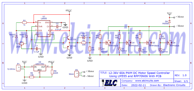
- 24W Stereo Hi-Fi Audio Amplifier using TDA2616 + PCB
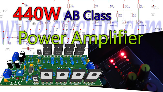
- 68W Hi-Fi Audio Power Amplifier using LM3886T IC + PCB
- 4 x 50W High Power Amplifier, 14.4V - IC TDA7563A + PCB
- 320W Power Audio Amplifier, Powered with 14.4V - 2Ω with IC TDA7560 + PCB
- 100W RMS Audio Amplifier IC TDA7294 + PCB
- 200W RMS Stereo Power Amplifier with IC STK4231II + PCB
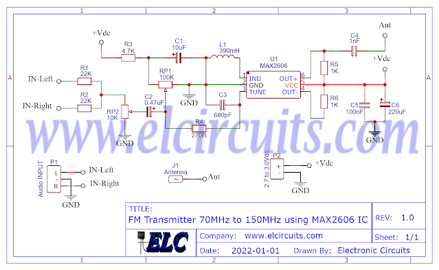
The Schematic Circuit
In Figure 2 below we have components arrangement of the power amplifier circuit with the LM3876 IC, and as we can see, the difficulty is not extreme.
Since there are few external components, making the amplifier circuit very simple to assemble, and a technician or hobbyist with medium experience can assemble it without much difficulty.
 |
| Fig. 2 - Schematic Circuit High Performance 56W Audio Power Amplifier using LM3876 IC |
It is important to remember to be careful when assembling the circuit, not to invert any component such as capacitor diodes, or even when connecting the symmetrical voltage of the power supply. Not to invert the voltage poles, because the integrated circuit or other components can be damaged.
The coil is formed is a 5uH coil, for those who are going to assemble it, you can assemble it with 10 turns of 18 AWG Wire with a 3/8" air core.
Components List
- Semiconductors
- U1 .............. LM3876 Integrated Circuit
- Resistors
- R1, R5 ....... 1K resistor (brown, black, red, gold)
- R2, R3 ....... 18K resistor (brown, gray, orange, gold)
- R4 .............. 10K resistor (brown, black, orange, gold)
- R6, R7 ....... 22K resistor (red, red, orange, gold)
- R8 .............. 100Ω resistor (brown, black, brown, gold)
- R9 .............. 10Ω / 1W resistor (brown, black, black, gold)
- RP1 ............ 10K Potentiometer
- Capacitors
- C1 ................. 2.2μF Ceramic/Polyester Capacitor
- C2 ................. 220pF Ceramic/Polyester Capacitor
- C3 ................. 47 Ceramic/Polyester Capacitor
- C4, C5 .......... 22μF / 65V Electrolytic Capacitor
- C6, C7, C8 .... 0.1uF Ceramic/Polyester Capacitor
- C9, C10 ......... 2.200uF / 65V Electrolytic Capacitor
- L1 .................. Inductor 5uH *Ver Texto
- Others
- P1, P2 ............ Screw Terminal Type 5mm 2-Pin Connector
- P3 .................. Screw Terminal Type 5mm 3-Pin Connector
- J1 ....................Set of male connectors 2-Pin (Optional)
- Other .............. PCB, Wires, Speaker, Heat Sink, etc.
Power Supply
You can in the link below:
 |
| Fig. 3 - Symmetrical Power Supply for Power Amplifiers |
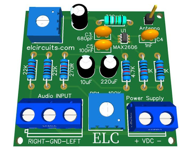
Printed Circuit Board
In Figure 3, we provide the PCB - Printed Circuit Board, in GERBER, PDF and PNG files. These files are available for free download, on the MEGA server, in a direct link, without any bypass.
All to make it easier for you to do a more optimized assembly, either at home, or with a company that prints the board. You can download the files in the Download option below.
 |
| Fig. 4 - PCB - High Performance 56W Audio Power Amplifier using LM3876 IC |
Files to download, Direct Link:
If you have any questions, suggestions or corrections, please leave them in the comments and we will answer them soon.
Subscribe to our blog!!! Click Here - elcircuits.com!!!
My Best Regards!!!