 |
| Automatic Programmable 4.2V Battery Charge, Current up to 500mA using LTH7R IC |
Effortless Battery Charging: Build an Automatic Programmable 4.2V Charger with up to 500mA Current Using LTH7R IC and PCB
The LTH7R IC is a constant current or constant voltage base charger chip, mainly used for single cell lithium battery charging.
No external sensing resistor is needed, it has its internal power MOSFET structure, so no external reverse diode is needed.
The LTH7R IC has under temperature protection and control, it adjusts the charging current automatically to limit high temperature on the chip.
Its charging voltage is fixed at 4.2V, and the charging current can be adjusted by an external resistor.
When the float voltage is reached and the charging current drops to 1/10 of the defined circuit, the LTH7R IC automatically completes the charging process.
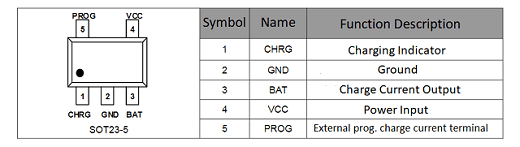 |
| Fig. 2 - Pinout LTH7R IC |
When the input source voltage is removed, the LTH7R IC automatically enters low current mode, drawing less than 2uA from the battery.
You may be interested in:
- 3.7V Li-Ion Battery Charger Circuit using MCP73831 IC + PCB
- Simple 12V battery charger with automatic charging indicator + PCB
- Lithium (Li-Ion) Battery Charger using LP2951 IC + PCB
- 12 Volts Automatic Lead Acid Battery Charger Using LM350 IC with PCB
- How To Make Rechargeable Emergency LED Light Using LM350 IC with PCB
- USB 5V 4A Car Charger using 78S05 with PCB
When the LTH7R IC enters standby mode, the supply current is less than 25uA. The LTH7R IC can also monitor charging current, has the features of voltage detection, auto-cycle charging, and has an indicator pin to indicate end-of-charge status and input voltage status.
Features
- Programmable charging current up to 500mA
- No need for external MOSFET, sensing resistor, reverse diode
- Constant current or constant voltage mode operation, with thermal protection function Preset charging voltage
- Standby current is 20uA
- 2.9V slow charge voltage
- Soft start limits the inrush current
- Adopt SOT23-5 package, application line
Product application
- Microphone Battery
- Light Camera
- Mobile Phones, PDAs, MP3 players
- Bluetooth headsets
External programming of the load current:
PROG (pin 5): Constant current load current setting and load current monitoring terminal. The load current can be programmed by connecting an external resistor from the PROG pin to ground.
In the pre-charge phase, the voltage of this pin is modulated by 0.1V; in the constant current charging stage, the voltage of this pin is fixed at 1V.
In all charging state modes, measuring the voltage of this pin can estimate the charging current according to the following formula:
General Formula:
I_bat = 1000 / R_prog
To use, for example, in a charger whose required current is 300mA, we can use the formula as follows:
- I_bat = 1000/ R_prog
- R_prog = 1000 / I_bat
- R_prog = 1000 / 300
- R_Prog = 3.3K
To use, for example, in a charger whose current required is the maximum current, 500mA, we can use the formula as follows:
- I_bat = 1000/ R_prog
- R_prog = 1000 / I_bat
- R_prog = 1000 / 500
- R_Prog = 2K
We leave just below a small table ready with five models with the standard currents for the battery charger.
| Model | R_prog | I_bat |
| 1 | 10K | 100mA |
| 2 | 5K | 200mA |
| 3 | 3,3K | 300mA |
| 4 | 2,5K | 400mA |
| 5 |
2K |
500mA
|
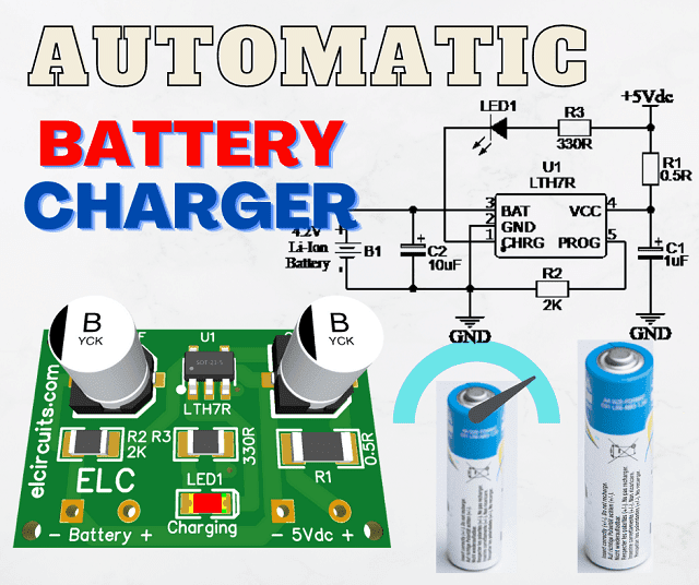
The Circuit Schematic
In Figure 3, below, we can see the schematic diagram of the Automatic Programmable 4.2V Battery Charge, Current up to 500mA using LTH7R IC.
All circuit components are SMD, the power supply input is done by soldering on the PCB. This type of miniaturized SMD circuit is great to be implemented in circuits with small spaces.
The capacitors are SMD electrolytic, but if you have tantalum capacitors, you can put them on, it will help with the plate height, but if you can't find them, you can use electrolytic.
The charger circuit supports voltage between 4.4V to 7V, the recommended is 5V, which is great news for us to be able to charge our battery in a PC USB port or even with cell phone chargers.
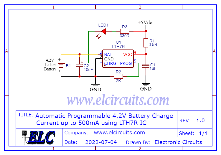 |
| Fig. 3 - Automatic Programmable 4.2V Battery Charge, Current up to 500mA using TH7R IC |
Printed Circuit Board
In Figure 4, we provide the PCB - Printed Circuit Board, in GERBER, PDF and PNG files. These files are available for free download, on the MEGA server, in a direct link, without any bypass.
All to make it easier for you to do a more optimized assembly, either at home, or with a company that prints the board. You can download the files in the Download option below.
 |
| Fig. 4 - PCB Automatic Programmable 4.2V Battery Charge, Current up to 500mA using TH7R IC |
Files to download, Direct Link:
Click on the link beside: GERBER, PDF and PNG files
I hope you enjoyed it!!!
If you have any questions, suggestions or corrections, please leave them in the comments and we will answer them soon.
Subscribe to our blog!!! Click here - elcircuits.com!!!
My Best Regards!!!