Wednesday, March 16, 2022

How To Make Rechargeable Emergency LED Light Using LM350 IC with PCB

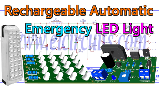
Fig. 1 - How To Make Rechargeable Emergency LED Light Using LM350 IC with PCB

Crafting a Rechargeable Emergency LED Light with LM350 IC: Step-by-Step Guide with PCB Implementation

You know that night when the power grid collapses and the power goes out, so we need a light to illuminate the darkness.

That's when we realized that we would need some equipment that could light up that darkness...

In this article, we are going to assemble a Rechargeable Automatic Emergency LED Light circuit that when the power goes out, it activates the set of LED lamps automatically using a rechargeable 12V battery.

You may be interested in: 

How the Circuit works

The Automatic Illuminator circuit is divided into three distinct parts:

The first part:

It's pretty obvious, we have the 220Vac or 110Vac voltage coming from the mains, and we need to convert it to 12Vac. For this, we use a 220V/12Vac transformer. The output of the 12Vac transformer, it is connected to a diode bridge to rectify the AC voltage to DC, and the 2200uF capacitor to filter this voltage.

The second part:

It is a 12V battery charging stage, it works simply as a charger, it has a status LED that when charging it stays on, and when charged the LED goes off.

The circuit uses the LM350T voltage regulator. The output current of the LM350 is 3 amps, it is necessary to adjust the output voltage through the trimpot of 4.7K, this voltage must be adjusted according to the battery used.

In some batteries this voltage is 13.8V, in others it is 14.4V, this is always described together in the general battery information.

For those who follow us here on our site, you may have already noticed that the 12V battery charger circuit is very similar to an article that we have already done here on our site, you can check it out by clicking on this link.

The Third part:

It is a control circuit composed of a BD140 PNP transistor, which works as a drive circuit, when there is power on the grid.

The voltage from the source passes through the 1K base current limiting resistor, and causes the transistor to stay open, keeping the light off, as soon as the voltage is cut off. 

The transistor as a switch closes the circuit, slinging the battery to the set of 20 LEDs, turning the light on.

The Circuit Diagram

The complete schematic diagram of the power supply is shown below in Figure 2, it is a simple but complete adjustable symmetric power supply.

Fig. 2 - Schematic Diagram Rechargeable Emergency LED Light Using LM350 IC

The Power Transformer

The transformer should have as primary according to your local network, 110Vac or 220Vac. The secondary should be 12V, since when we pass through the rectification, this 12Vac voltage is transformed more or less into 16.9Vdc.

The transformer should have a current of 3 amps, in case you are going to use it with large batteries, such as 7A, 9A, etc… 

If you are going to work with smaller batteries, it is up to you to place a transformer proportional to the total power of the LEDs and the battery used. The transformer configuration diagram is shown in Figure 4 below.

Fig. 3 - Schematic Diagram Transformer 110/220Vac to 12Vac 3Amps

Component List

  • Semiconductors
    • U1 ........................ LM350 Voltage Regulator  
    • Q1 ........................ BC548 NPN Transistor
    • Q2 ........................ BD140 PNP Transistor
    • D1 ........................ KBU4A - 4A Rectifier Bridge
    • D2 ........................ 1N5408 Diode Rectifier 
    • LED1 to LED20 ... Light Emitter Diode 5mm High Light
    • LED1 .................... Light Emitter Diode 3mm (general use)

  • Resistors
    • R1 ............... 100Ω 1/8w Resistor (brown, black, brown, gold
    • R2 ............... 0.5Ω 5W Resistor (green, black, silver, gold)
    • R3 ............... 470Ω 1/8w Resistor (yellow, violet, brown, gold
    • R4 ............... 120Ω 1/8w Resistor (brown, red, brown, gold
    • R5 ............... 1kΩ 1/8w Resistor (brown, black, red, gold
    • R6 to R10 ... 1Ω 3W Resistor (brown, black, black, gold)
    • RP1 ............. 4K7Ω Trimmer

  • Capacitors
    • C1 ...... 2.200uF - 25V Electrolytic capacitor 
    • C2 ...... 0.33uF - 25V Electrolytic capacitor 

  • Miscellanies
    • P1, P2 ....... Connector 2 screw terminal 5mm 2 Pins
    • T1 ............. Transformer Reduction 110/220ac to 12Vac (See Text)
    • Others ....... Wires, Solders, pcb, heat sink, etc.

PCB - Download

We provide the files with the PCB, the schematic, the PDF, GERBER and JPG, PNG and provide a direct link for free download and a direct link, "MEGA".

Fig. 4 - PCB - Rechargeable Emergency LED Light Using LM350 IC

Click on the direct link to download the files: Layout PCB, PDF, GERBER, JPG

I hope you enjoyed it!!!

If you have any questions, suggestions or corrections, please leave them in the comments and we will answer them soon.

Subscribe to our blog!!! Click here - elcircuits.com!!!

My Best Regards!!!

Sunday, March 6, 2022

1.5V to 28V, 7.5 Amps Adjustable Symmetric Power Supply using IC LT1083 with PCB

Fig.1 - 1.5V to 28V, 7.5 Amps Adjustable Symmetric Power Supply using IC LT1083 with PCB

Versatile Power at Your Fingertips: Build an Adjustable 1.5V to 28V, 7.5 Amps Symmetric Power Supply with IC LT1083 and PCB

This is a power supply designed to be used in a technical bench, based on the LT1083 integrated circuit, which is an adjustable 3-terminal positive voltage regulator.

Which provides a current of 7.5A in a variable output voltage range of 1.5 to 28V, and even has short circuit and over temperature protection.

The Circuit provides a symmetrical output, which pleases all of us engineers, technicians and designers, this type of power supply, as it brings us great efficiency for application in technical benches, mainly for testing audio amplifiers.

LT1083 IC Description

The  LT1083  positive  adjustable  regulator  is designed to provide  7.5A with higher efficiency than currently  available  devices. 

In Figure 2 - You'll find the description of the input, output and ground pins. There are other types of encapsulation, as this TO - 3P is the most common.

Fig. 2 - Pinout LT1083

All  internal  circuitry  is designed to operate down to 1V input to output differential, and the dropout voltage is fully specified as a function of load current.

Dropout is guaranteed at a maximum of 1.5V at  maximum  output  current,  decreasing  at  lower  load currents. 

On-chip trimming adjusts the output voltage to 1%. The current limit is also trimmed, minimizing the stress on both the regulator and power source circuitry under overload conditions.

The LT1083  series  devices  are  pin  compatible  with  older three terminal  regulators. A 10μF  output  capacitor  is required on these new devices; however, this is usually included in most regulator designs.

Unlike  PNP  regulators,  where  up  to  10%  of  the  output current is wasted as quiescent current, the LT1083 quiescent current flows into the load, increasing efficiency.

Features

  • Three-Terminal 3.3V, 3.6V, 5V, 12V or Adjustable
  • Output Current of 3A, 5A or 7.5A
  • Operates Down to 1V Dropout
  • Guaranteed Dropout Voltage at Multiple Current Levels
  • Line Regulation: 0.015%
  • Load Regulation: 0.1%
  • 100% Thermal Limit Functional Test
  • Adjustable Versions Available

How the Circuit Work

The circuit operation is quite simple, and its operation is applied with an artifice that we did to join two adjustable power sources into one.

Since we don't have "as far as I know", a regulator of the same negative line, like what happens with the regulators LM317, LM7812 and etc.

The bridges of diodes KBPC5010 D1 and D4, are responsible for rectifying the circuit, this diode bridge is able to support currents up to 50A

I know it's an exaggeration, but it was what I had here, you can be putting with lower current, as the KBPC1510, for 15A, or the KBPC1010 for 10A.

The capacitors C1 and C3, are electrolytic capacitors responsible for filtering the circuit, we use them of 10,000uF, but if you don't have one you can put one of 8,000uF. Remembering that they have to be able to avoid Ripple in the power supply.

The resistors R1 and R3 are the limiters for LED1 and LED2, which are used as voltage signaling for the two sources.

The voltage that comes already rectified and filtered enters the Positive Voltage Regulators, as we can see in the circuit, they are identical circuits, and through the double potentiometer the output voltage regulation is done, ranging from 1.5V to 28V.

The diodes D2, D3, D5, and D6, are for reverse voltage protection that can arise from the circuit and damage the Regulators, and the diodes protect these voltages in the regulators.

The resistors R2 and R4, are responsible for the Feedback voltage, or feedback, they keep the output voltage stable, they are resistors that if you have conditions, put the ones with low error percentage, such as precision resistors with 1%.

And finally, the capacitors C2 and C4, are for spurious filter, if you can afford it, it is preferable tantalum capacitors. 

The Circuit Diagram

The complete schematic diagram of the power supply is shown below in Figure 2, it is a simple but complete adjustable symmetric power supply.

Fig. 3 - Schematic Diagram 1.5V to 28V, 7.5 Amps Adjustable Symmetric Power Supply using IC LT1083 

The Power Transformer

The transformer must be symmetrical with center tape open, this means that it will to have two independent winding: "2 Wire + 2 Wire", as illustrated in Figure 4 below. 

Fig. 4 - Symmetrical Transformer with Independent secondary winding

The transformer must be able to supply 8A at the symmetrical output. The primary voltage, “input voltage”, must correspond to the voltage in your area; 110V or 220Vac

The secondary voltage, “output voltage”, should be 21Vac in each coil, because after rectification it will supply the circuit with 30Vdc.

Component List

  • Semiconductors
    • U1, U2 .................. LT1083 Voltage Regulator  
    • D1, D4 .................. KBPC5010 - 50A Rectifier Bridge *See Text
    • D2, D3, D5, D6 .... 1N4007 Diode Rectifier 
    • LED1, LED2 ........ Light Emitter Diode (General Use)

  • Resistors
    • R1, R3 ....... 2K7Ω 1/8w Resistor (red, violet, red, gold
    • R2, R4 ....... 120Ω 1/8w Resistor (brown, red, brown, gold
    • RP1 ........... 5KΩ Double Potentiometer 

  • Capacitors
    • C1, C3 ........ 10.000uF - 45V Electrolytic capacitor 
    • C2, C4 ........ 10uF - 45V Electrolytic capacitor 

  • Miscellanies
    • P1, P2 ........ Connector 2 screw terminal 5mm 2 Pins
    • P3 .............. Connector 3 screw terminal 5mm 3 Pins
    • Others ....... Wires, Power Transformer, Solders, pcb, heat sink, etc.

Printed Circuit Board - Download

We provide the files with the PCB, the schematic, the PDF, GERBER and JPG, PNG and provide a direct link for free download and a direct link, "MEGA".

Fig. 5 - PCB - 1.5V to 28V, 7.5 Amps Adjustable Symmetric Power Supply using IC LT1083

Click on the direct link to download the files: Layout PCB, PDF, GERBER, JPG

I hope you enjoyed it!!!

If you have any questions, suggestions or corrections, please leave them in the comments and we will answer them soon.

Subscribe to our blog!!! Click here - elcircuits.com!!!

My Best Regards!!!

Monday, February 28, 2022

25A - 110/220V Solid State Relay (SSR) Circuits using Triac BTA24-600 With PCB

Fig. 1 - 25A - 110/220V Solid State Relay (SSR) Circuits using Triac BTA24-600 With PCB

Efficient Power Control: Building 25A - 110/220V Solid State Relay (SSR) Circuits with Triac BTA24-600 and PCB

Solid State Relays (SSR) are nothing new, but making your own SSR is priceless! With it we can connect to digital control devices such as; Arduino, PIC, ESP, CLP, Raspberry, etc.

Besides that, we can spend a fraction of the price of a commercial relay if we make our own SSR relay, and still have in our hands the control that if something goes wrong, we can repair it without too much trouble.

The Solid State Relay

Solid State Relay is similar to switching relays, they all function as a switch that is controlled by an input voltage or current, isolated from the output.

The basic difference is that Solid State Relay, or (SSR), has no moving parts, but uses the electrical and optical properties of solid-state semiconductors.

Electromechanical Relays (EMR), on the other hand, use coils, magnetic fields, springs, and mechanical contacts to operate and switch through a supply voltage.

Our circuit uses few external components, and is easy to assemble, the components are easy to acquire in the market, and basically there are two:

  • The isolation circuit formed by the MOC3041optical isolator.
  • The power control formed by the BA24-600 TRIAC, they will be explained  just below.   

CAUTION!!!

This circuit works directly connected to the 110/220V electrical network, and has a high power load, any carelessness, or wrong connections, error in the project, or any other occasion, can lead to irreversible damage.

We are not responsible for any type of event. If you do not have enough experience to assemble this circuit, do not do it, and if you do, when testing, be sure to have the proper protections and be accompanied by someone else.

BTA24 Description 

Available either in through-hole or surface-mount packages, the BTA24 TRIAC is suitable for general purpose AC switching.

They can be used as an ON/OFF function in applications such as static relays, heating regulation, induction motor starting circuits... or for phase control operation in light dimmers, motor speed controllers.

The snubber-less versions (BTA/BTB...W and T25 series) are specially recommended for use on inductive loads, thanks to their high commutation performances. 

By using an internal ceramic pad, the BTA series provides voltage insulated tab (rated at 2500V RMS) complying with UL standards.

6-Pin  DIP  Zero-Cross Opto-isolators  Triac  Driver  Output

(400 Volts Peak)

The MOC3041, MOC3042 and MOC3043 devices consist of gallium arsenide infrared  emitting  diodes  optically  coupled  to  a  monolithic  silicon  detector performing the function of a Zero Voltage Crossing bilateral triac driver.

They  are  designed  for  use  with  a  triac  in  the  interface  of  logic  systems  to equipment powered from 115/220 Vac  lines,  such  as  solid–state  relays,  industrial controls, motors, solenoids and consumer appliances, etc.

  • Simplifies Logic Control of 115 Vac Power
  • Zero Voltage Crossing
  • dv/dt of 2000 V/μs Typical, 1000 V/μs Guaranteed

We are using the MOC3041 optical isolator, because of this model, having a zero-crossing SSR accepts triggering at any time, but delays the triggering of the AC load until the next time the AC voltage passes zero volts.

This is useful to eliminate RFI (Radio Frequency Interference) and to prevent a large current from flowing to the load almost instantly. 

Solid State Relay Circuit 

The 25A - 110/220V Solid State Relay (SSR) Circuits using Triac BTA24-600 circuit diagram is shown in Figure 2 below.

It uses a 25 Amp TRIAC BTA24-600, this is enough to handle loads up to a little over 5.500W, obviously using a isolated heat sink.

Fig. 2 - 25A - 110/220V Solid State Relay (SSR) Circuits using Triac BTA24-600

Basic Components Function

  • Diode D1, is used for reverse voltage protection, it inhibits reverse voltage. 

  • Resistor R1 of 240 ohm, limits the input current to the internal LED of the MOC

  • Resistor R2 of 330 ohms for 1W, it serves to limit the supply current to the MOC's internal DIAC.

  • Resistor R3 of 56 ohm, prevents any di/dt current when the TRIAC is off, eliminating false triggering. 

Components List

  • Semiconductors
    • Q1 .... BTA24-600 Triac
    • U1 .... MOC 3041 opto-isolator
    • D1 .... 1N4007 Diode

  • Resistor
    • R1 .... 240Ω (red, yellow, brown, gold)
    • R2 .... 330Ω (orange, orange, brown, gold)
    • R3 .... 56Ω (green, blue, black, gold
  • Miscellaneous 
    • P1, P2 .... 2-pin PCB soldering terminal blocks (Optional)
    • Others .... PCB, heat sink, wires, etc.

Printed Circuit Board

We are offering the PCB - Printed Circuit Board, in GERBER, PDF and PNG files, for you who want to do the most optimized assembly, either at home.

If you prefer in a company that develops the board, you can is downloading and make the files in the Download option below.

Fig. 3 - PCB - 25A - 110/220V Solid State Relay (SSR) Circuits using Triac BTA24-600

Files to Download, Direct Link:

I hope you enjoyed it!!!

If you have any questions, suggestions or corrections, please leave them in the comments and we will answer them soon.

Subscribe to our blog!!! Click here - elcircuits.com!!!

My Best Regards!!!

Saturday, February 26, 2022

4A Low-Noise High-Frequency Step-Up DC-DC Converter using MAX1709 with PCB

Fig. 1 - 4A Low-Noise High-Frequency Step-Up DC-DC Converter using MAX1709 with PCB

This is a DC-DC converter circuit that uses a MAX1709 series Integrated Circuit as the main component, it works with a Step-Up conversion system.

This powerful microcircuit is able to work with very few external components and deliver a fixed 3.3V or 5V or adjustable 2.5V to 5.5V voltage, with 4 Amperes of output current.

Integrated Circuit General Description

The MAX1709 sets a new standard of space savings for high-power,  step-up  DC-DC  conversion.  It  delivers  up to  20W  at  a  fixed  (3.3V  or  5V)  or  adjustable  (2.5V  to5.5V)  output,  using  an  on-chip  power  MOSFET  from  a +0.7V to +5V supply. 

Fixed-frequency PWM operation ensures that the switching noise spectrum is constrained to the 600kHz fundamental and its harmonics, allowing easy post filtering  for  noise  reduction.  

External  clock  synchronization capability  allows  for  even  tighter  noise  spectrum  control. Quiescent power consumption is less than 1mW to extend operating time in battery-powered systems. 

Two  control  inputs  (ONA ONB)  allow  simple  push-on, push-off  control  through  a  single  momentary  push button  switch,  as  well  as  conventional  on/off  logic  control. 

The  MAX1709  also  features  programmable  soft-start and current limit for design flexibility and optimum performance with batteries. 

The maximum RMS switch cur-rent  rating  is  10A.  For  a  device  with  a  lower  current rating, smaller size, and lower cost, refer to the MAX1708 datasheet.

The Circuit Schematic

In Figure 2, below, we can see the schematic diagram of 4A Low-Noise High-Frequency Step-Up DC-DC Converter using MAX1709.

The circuit is simple to assemble, there are few external components, and there is no need for adjustment, once assembled, it is ready to work, if everything is correct, of course!

The PCB tracks are bent, the main ones have their tracks at the bottom and at the top of the PCB, because the current is 4 amperes.

The capacitors are tantalum, however if you can't find them, electrolytic capacitors can be used, however for more sensitive circuits, the performance may not be as expected, but in most circuits they work very well.

The DC-DC converter supports input from 0.7V up to 5V, and at the output it maintains the stabilized voltage of 5V, however to get the promised 4 Amps, it is necessary to have at least 3.3V at the input.
Fig. 2 - Schematic Circuit 4A Low-Noise High-Frequency Step-Up DC-DC Converter using MAX1709

Components List

  • Semiconductors
    • U1 ...... MAX1709 SMD Integrated Circuit
    • D1 .....  B520C SMD Schottky Diode 5A

  • Resistor
    • R1 ..... 312KΩ SMD resistor (orange, brown, red, orange, gold
    • R2 ..... 2Ω SMD resistor (red, black, black, gold)
  • Capacitor
    • C1, C2, C6, C7 ... 150uF SMD Tantalum Capacitor
    • C3 ....................... 10nF SMD Ceramic Capacitor
    • C4 ....................... 220nF SMD Ceramic Capacitor
    • C5 ....................... 100nF SMD Ceramic Capacitor

  • Miscellaneous 
    • L1 .......... 1uH 5A SMD Inductor
    • P1, P2 .... 2-pin PCB soldering terminal blocks (Optional)
    • Others .... Printed Circuit Board, wires, etc.

Printed Circuit Board

In Figure 3, we provide the PCB - Printed Circuit Board, in GERBER, PDF and PNG files. These files are available for free download, on the MEGA server, in a direct link, without any bypass. 

All to make it easier for you to do a more optimized assembly, either at home, or with a company that prints the board. You can download the files in the Download option below.
Fig. 3 - PCB - 4A Low-Noise High-Frequency Step-Up DC-DC Converter Using MAX1709

Files to download, Direct Link:

Click on the link beside: GERBER, PDF and PNG files

If you have any questions, suggestions or corrections, please leave them in the comments and we will answer them soon.

Subscribe to our blog!!! Click Here - elcircuits.com!!!

My Best Regards!!!

Friday, February 25, 2022

3500W Dimmer for 110V or 220V using TRIAC TIC246 with PCB

Fig. 1 - 3500W Dimmer for 110V or 220V using TRIAC TIC246M with PCB

This is a dimmable load controller circuit, its operation is based on the control of the sine cycle, keeping it off during a small period of the wave. And work only for a specific part of the wave keeping the load with part of the wave controlled by period, similar to PWM.

With this type of circuit we can control the intensity of an incandescent light, ceiling fans, resistive load, among others, through the decay of the cycle regulated through a potentiometer.

The Dimmer Circuit 

The 3500W Dimmer for 110V or 220V using TRIAC TIC246M with PCB circuit diagram is shown in Figure 2 below. 

It uses a 16 Amp TRIAC TIC246, this is enough to handle loads up to a little over 3500W, obviously with heat sink.
Fig. 2 – Schematic Circuit 3500W Dimmer for 110V or 220V using TRIAC TIC246M


If you need to increase the power of the circuit, you can replace the thyristor in the circuit. Using the simple formula of Ohms Law, P = V * I, through current and voltage, we can find the power of the circuit with each of the Thyristors:
  • TIC246 = 16A:
    • At 110V => P = 110 * 16 = 1760W
    • At 220V = P = 220 * 16 = 3,520W

  • TIC256 = 20A:
    • At 110V => P = 110 * 20 = 2,200W
    • At 220V => P = 220 * 20 = 4,400W

  • TC266 = 25A:
    • At 110V => P = 110 * 25 = 2750W
    • At 220V => P = 110 * 25 = 5,500W

CAUTION!!!

This circuit works directly connected to the 110/220V electrical network, and has a high power load, any carelessness, or wrong connections, error in the project, or any other occasion, can lead to irreversible damage. 

We are not responsible for any type of event. If you do not have enough experience to assemble this circuit, do not do it, and if you do, when testing, be sure to have the proper protections and be accompanied by someone else.

How it works

When we connect the AC mains to the circuit, there is a charging of the capacitor C4 through the voltage set in the Trimpot RP1. When biased, there is a sending of this voltage to the DIAC through the current limiting resistor R3

The DIAC is a bidirectionally biased diode, and is triggered when it reaches its breakdown voltage, about 30V, as it is connected to the Gate of the TRIAC. As soon as it reaches its breakdown voltage, both positive and negative pulses are activated in the Gate of the TRIAC

However, this also charges the capacitor with reverse voltage from the negative half-cycle, and in this charging time the TRIAC stays open until the cycles compound.

This is repeated with each cycle of the AC sine wave signal from the grid, which maintains its drive and cut cycle repeatedly, leading to an output voltage lower than that of the input.

The network formed by capacitor C1 and coil L1 works as a filter to inhibit RF spurious propagation through the power network. While R1 and C2 are employed for transient reductions.

The network formed by C4 and R5 in parallel with the TRIAC, serves to prevent the TRIAC from burning out, because when the dimmer is controlling inductive loads, reverse voltage spikes are formed at the moment of switching. 

Thus, the capacitor absorbs the generated overvoltage and the resistor limits the discharge current from the capacitor onto the TRIAC.

The resistor R4 connected in parallel, is used to decrease the ohmic rating of variable resistor RV1, since the applicable value for RV1 is 150k ohms.

Since it is not easy to find this variable resistor, we made an association of resistors to get it close to 150k ohms.

The network formed by capacitor C1 and coil L1 works as a filter to inhibit RF spurious propagation through the power network.

The L1 coil consists of a small ferrite rod, 1/4" diameter and 11/4" long, wound with 55 turns of 28 SWG enameled copper wire.

You can be using the ferrite coil from a PC power supply to make your coil, or you can be buying a commercial 40uH coil. 

Components List

  • Semiconductors
    • U1 .............. TIC246 Triac *See Text
    • D1 .............. DB-3 DIAC Diode

  • Resistor
    • R1 ................ 56Ω (green, blue, black, gold
    • R2 ................ 2K2Ω (red, red, red, gold)
    • R3 ................ 5K6Ω (green, blue, red, gold)
    • R4 ................ 390Ω  (orange, white, brown, gold)
    • R5 ................ 250KΩ Potentiometer
  • Capacitor
    • C1, C2, C4 .... 100nF / 600V Polyester Capacitor 
    • C3 ................. 47nF Ceramic/Polyester Capacitor

  • Miscellaneous 
    • P1, P2 ......... 2-pin PCB soldering terminal blocks
    • F1 ................ Fuse 15A with soldering terminal blocks
    • L1 ................ 40uH Inductor *See Text
    • Others ......... PCB, heat sink, wires, etc.

Printed Circuit Board

We are offering the PCB - Printed Circuit Board, in GERBER, PDF and PNG files, for you who want to do the most optimized assembly, either at home.

If you prefer in a company that develops the board, you can is downloading and make the files in the Download option below.
Fig. 3 - PCB - 3500W Dimmer for 110V or 220V using TRIAC TIC246M with PCB

Files to download, Direct Link:


If you have any questions, suggestions or corrections, please leave them in the comments and we will answer them soon.

Subscribe to our blog! Click Here - elcircuits.com!

My Best Regards!!!


Wednesday, February 23, 2022

160W High Fidelity Amplifier using Mosfet 2SK1058 and 2SJ162 with PCB

Fig. 1- 160W High Fidelity Amplifier using Mosfet 2SK1058 and 2SJ162 with PCB

This is a High Fidelity power amplifier, which uses 2 pairs of complementary MOSFETs output transistors, 2SK1058 and 2SJ162, which gives us a 160W power output. 

The circuit is simple to assemble, assuming you have advanced knowledge in electronics, you will be able to assemble this circuit without too much difficulty.

Basic operation of the circuit

This amplifier has a few many steps, and we could break down each component, but it would certainly be too long, so let's explain the main stage of the amplifier process. 

The 160W High Fidelity Amplifier circuit diagram is shown in Figure 2 below. It uses 4 output Mosfet power transistors, 2 transistors for the positive cycle and 2 transistors for the negative cycle.
Fig. 2 - Schematic Circuits 160W High Fidelity Amplifier using Mosfet 2SK1058 and 2SJ162

We will start with first Stage: 

It is formed by a pair of MPSA56 PNP transistors, they form the input of the differential amplifier. 
The main characteristic is to amplify the difference of the input signals without amplifying the common mode signal.

In the second stage:

We have two pairs of transistors, 2 NPN BD139 transistors and 2 PNP TIP140 transistors, they constitute a differential current source pair formed by the BD139 transistors pair. And with a current mirror formed by the BD140 transistors pair, in Cascade mode creating a telescopic amplifier stage.

In the third stage:

It is formed by the 4 Output MOSFETs transistors, two N-channel type transistors 2SK1058 and other two P-channel type transistors 2SJ162. They receive the signal from stage 2 which is a module in Cascade, as already explained, and deliver to the output load, formed by the speaker.

The output transistors should be equipped with a Heat Sink, and should be electrically separated with thermal insulators.

Power Supply

The power supply is a symmetrical source, +Vdc GND -Vdc, and must contain a current capable of supporting the total power of the Amplifier.

If the circuit is used in MONO mode "One channel", the recommended current is 4 Amperes. If a STEREO version "Two channels" is used, the current should be doubled to 8 Amperes.

The amplifier work voltage is ±45Vdc SYMMETRICAL, to be used with an output load between 4 to 8 ohms.

In Figure 3 below, we have a suggestion for a power supply that we use in our projects. In this article, besides having the schematic diagram with the Printed Circuit Board, you will understand how to easily calculate your own Power Supply, with the desired voltage.

You can in the link below:

Fig. 3 - Symmetrical Power Supply for Power Amplifiers

Components List

  • Semiconductors
    • Q1 .......................... MPSA56 PNP Transistor
    • Q3, Q4 ................... BD139 NPN Transistor
    • Q5, Q6 ................... BD140 PNP Transistor
    • Q7, Q8 ................... 2SK1058 N-Channel Mosfet Transistor
    • Q9, Q10 ................. 2SJ162 P-Channel Mosfet Transistor
    • D1, D2 ................... 1N4007 Diode

  • Resistor
    • R1, R2, R10 ................ 47KΩ (yellow, violet, orange, gold
    • R3, R4 ........................ 3K3Ω (orange, orange, red, gold)
    • R5 ............................... 1K2Ω  (brown, red, red, gold)
    • R6 ............................... 10KΩ  (brown, black, orange, gold)
    • R7, R8 ........................ 1KΩ (brown, black, red, gold)
    • R9 ............................... 2K2Ω (red, red, red, gold)
    • R11, R12, R13, R14 ... 47Ω (yellow, violet, black, gold)
    • R15, R16, R17, R18 ... 022Ω (red, red, silver, gold)
    • R19 ............................. 10Ω (brown, black, black, gold)
  • Capacitor
    • C1 ........................ 4.7uF / 65V Electrolytic Capacitor 
    • C2, C4, C5 ........... 470pF Ceramic Capacitor
    • C3 ........................ 47uF / 65V Electrolytic Capacitor 
    • C6 ........................ 100nF Ceramic Capacitor

  • Miscellaneous 
    • P1, P2 .......... 2-pin PCB soldering terminal blocks
    • P3 ................ 3-pin PCB soldering terminal blocks
    • Others ......... PCB, heat sink, power supply, wires, etc.


We are offering the PCB - Printed Circuit Board, in GERBER, PDF and PNG files, for you who want to do the most optimized assembly, either at home.

If you prefer in a company that develops the board, you can is downloading and make the files in the Download option below.

Fig. 3 - PCB 160W High Fidelity Amplifier using Mosfet 2SK1058 and 2SJ162

Files to download, Direct Link:


If you have any questions, suggestions or corrections, please leave them in the comments and we will answer them soon.

Subscribe to our blog!!! Click Here - elcircuits.com!!!

My Best Regards!!!