 |
| Fig. 1 - High Fidelity 14W - 12V Power Amplifier using TDA2030 IC |
The TDA2030 is a monolithic integrated circuit in a Pentawatt® package, intended to be used as a low frequency Class AB amplifier.
Typically, it provides output power of 14W (d = 0.5%) at 14V / 4Ω; at ± 14V the guaranteed output power is 12W with a load of 4Ω and 8W on an 8Ω.
In Figure 2, we can see the pinout of the TDA2030, it provides a high current output and very low harmonic and cross distortion.
 |
| Fig. 2 - Pinout TDA2030 |
In addition, the device incorporates a short-circuit protection system and an arrangement to automatically limit the dissipated energy so as to keep the working point of the output transistors within their safe operating area. A conventional thermal shutdown system is also included.
You might also be interested in:
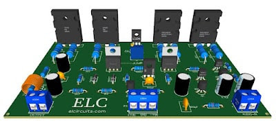
- 170W AB Class Bridge Mode Amplifier using TDA7294 IC + PCB
- HI-FI 120W RMS Amplifier Circuit using LM4780 IC + PCB
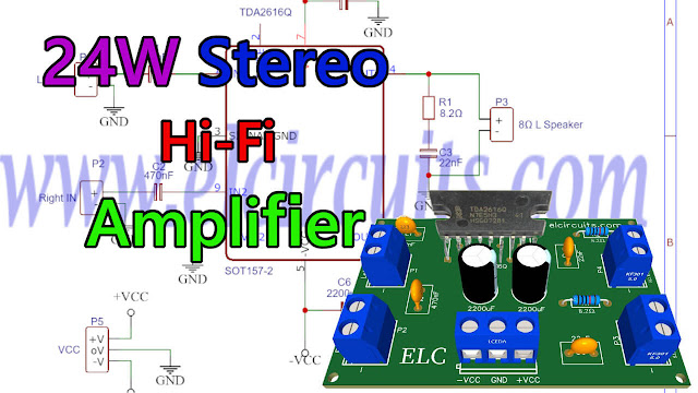
- 24W Stereo Hi-Fi Audio Amplifier using TDA2616 + PCB
- 68W Hi-Fi Audio Power Amplifier using LM3886T IC + PCB
- 4 x 50W High Power Amplifier, 14.4V - IC TDA7563A + PCB
- 320W Power Audio Amplifier, Powered with 14.4V - 2Ω with IC TDA7560 + PCB
- 100W RMS Audio Amplifier IC TDA7294 + PCB
- 200W RMS Stereo Power Amplifier with IC STK4231II + PCB
Features
- Wide-range supply voltage, up to 36 V
- Single power supply
- Short-circuit protection to ground
- Thermal shutdown
- Low distortion
PROTECTION AGAINST SHORT CIRCUIT
The TDA2030 has a unique circuit that limits current from the output transistors. the maximum output current is a function of the emitter-collector voltage; hence the output transistors work within their safe operating area.
This function can therefore be considered to be peak power limiting rather than simple current limiting. Reduces the possibility of the device being damaged during an accidental output short circuit.
THERMAL DISCONNECTION
The presence of a thermal limiting circuit offers the following advantages:
- An output overload (even if it is permanent), or an ambient temperature above the limit can be easily withstood as the Tj cannot exceed 150°C.
- The heat sink may have a lower safety factor compared to a conventional circuit. There is no possibility of damage to the device due to high junction temperature. If for some reason the junction temperature rises up to 150°C, thermal shutdown simply reduces power dissipation at current consumption.
The maximum allowable power dissipation depends on the size of the external heat sink (ie thermal resistance); this power is dissipated depending on the ambient temperature for different thermal resistance.
The schematic circuit is shown in Figure 3, it is a very simple circuit, which can be easily assembled even by people who are not experienced in circuit assembly.
 |
| Fig. 3 - Schematic High Fidelity 14W - 12V Power Amplifier using TDA2030 IC |
Component List
- Semiconductors
- U1 .................. TDA2030 Integrated Circuit
- D1, D2 ........... 1N4007 Silicon Diode
- Resistors:
- R1, R2, R3 ..... 100KΩ resistor (brown, black, yellow, gold)
- R4 .................. 4K7Ω resistor (yellow, red, purple, gold)
- R5 .................. 150KΩ resistor (brown, green, yellow, gold)
- R6 .................. 1Ω / 1W resistor (brown, black, gold, gold)
- RP1 ............... 22KΩ Potentiometer
- Capacitors
- C1 ................. 2.2µF / 35V Electrolytic Capacitor
- C2 ................. 22µF / 35V Electrolytic Capacitor
- C3 ................. 1000µF / 35V Electrolytic Capacitor
- C4 ................. 2µF / 35V Electrolytic Capacitor
- C5 ................. 100nF Polyester or Ceramic Capacitor
- C6.................. 220nF polyester or ceramic
- C7 ................. 2200µF / 35V Electrolytic Capacitor
- Others
- P1, P2, P3 ... Screw Terminal Type 5mm 2-Pin Connector
- Printed circuit board, heat sink, box, wires, etc.
In Figure 4, we are offering the PCB - Printed Circuit Board, in GERBER, PDF and PNG files, for you who want to do the most optimized assembly, either at home, or if you prefer in a company that develops the board, you can is downloading and make the files in the Download option below.
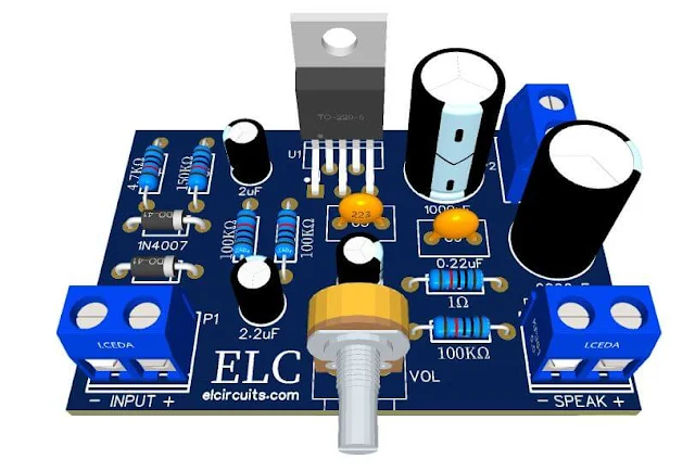 |
| Fig. 4 - PCB - High Fidelity 14W - 12V Power Amplifier using TDA2030 IC |
Files to Download, Direct Link:
If you have any questions, suggestions or corrections, please leave them in the comments and we will answer them soon.
Subscribe to our blog!!! Click Here - elcircuits.com!!!
My Best Regards!!!