Saturday, December 31, 2022

RJ45 Ethernet Cable Color Standard - T568A and T568B - EIA/TIA Standard

Demystifying RJ45 Ethernet Cable Color Standards: T568A vs. T568B in EIA/TIA Standard

Back in the past, a few decades ago, there were no standard regulations for the wiring of structured networks in the IT industry.

The standards for these networks were decided upon by the companies or professionals responsible for installing the wired networks. 

This lack of standardization made it difficult to maintain or modify the network structures of companies, especially when done by another company or professional.

To address this issue and with the increasing growth of technology and infrastructure for wired networks, the TIA/EIA standards were developed. 

In 1991, the TIA/EIA, 568A and 568B standards were introduced by the Electronic Industries Association (EIA) and the Telecommunications Industry Association (TIA) to standardize the electrical and electronic connections of network cables and their connections. 

The 568A standard was revised in 1994 to include Category 4 and Category 5 (UTP - Unshielded Twisted Pair) wiring, and in 2001 the EIA/TIA 568-B standard was published, covering a total of 10 different categories.

You may be interested in: 

T568A and T568B Categories

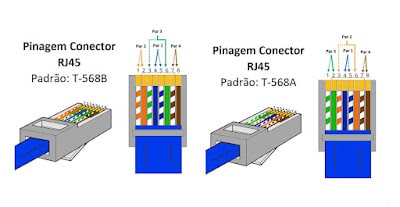
There are two different categories of TIA/EIA standards, commonly known as RJ45 Standard B and RJ45 Standard A, which are actually T568A and T568B.

These are termination standards used by Internet Providers, Backbone Infrastructure, Industrial Wiring Infrastructure, and also by small businesses and residential wiring.

However, the difference between these two categories is that the orange/white and green/white pairs, which correspond to pins 1 & 2, 3 & 6, are exchanged in the assembly of the cable, as illustrated in Figure 1 below.

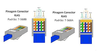
Fig.1-Standard-Colors-Cable-Network-RJ45-T-568A-T-568B-Standard-EIA/TIA

It is worth remembering that even with changes to the set of pairs, when the same standards are used at both ends of the cable, the results will be the same, with direct connections at their ends.

In Table 1 below, we have the configuration of the pins and their corresponding colors, following the two standards side by side for comparison.

Sequential Table of Colors and Pinning Standard T-568A and T-568B

PinT-568AT-568B
1White/GreenWhite/Orange
2Green        Orange
3White/OrangeWhite/Green
4BlueBlue 
5White/BlueWhite/Blue
6OrangeGreen
7White/BrownWhite/Brown
8BrownBrown

The T568A standard is the widely accepted standard because it is compatible with most wiring schemes and is what I recommend for most applications.

Crossover Cable

Crossover cables, use the T-568A and T-568B standards at each end as illustrated in Figure 2 below. These categories of cables are used when we need to, for example, connect two computers or laptops without using a router or switch.

Fig. 2 - Connection of Crossover Cable Standards T-568A and T-568B

It is worth remembering that if you are still using older equipment, you should not connect crossover cables between the computer and a switch or router, as in some cases it can damage the equipment.

Now if you work with newer, more modern equipment, they use AUTO MDI/MDIX technology, which automatically identifies the connected interface and even if it is of the crossover type, there is no problem, as it automatically configures itself.

I hope you enjoyed it!!!

If you have any questions, suggestions or corrections, please leave them in the comments and we will answer them soon.

Subscribe to our blog!!! Click here - elcircuits.com!!!

My Best Regards!!!

Monday, July 4, 2022

Automatic Programmable 4.2V Battery Charge, Current up to 500mA using LTH7R IC with PCB

Automatic Programmable 4.2V Battery Charge, Current up to 500mA using LTH7R IC

Effortless Battery Charging: Build an Automatic Programmable 4.2V Charger with up to 500mA Current Using LTH7R IC and PCB

The LTH7R IC is a constant current or constant voltage base charger chip, mainly used for single cell lithium battery charging.

No external sensing resistor is needed, it has its internal power MOSFET structure, so no external reverse diode is needed.

The LTH7R IC has under temperature protection and control, it adjusts the charging current automatically to limit high temperature on the chip.

Its charging voltage is fixed at 4.2V, and the charging current can be adjusted by an external resistor.
When the float voltage is reached and the charging current drops to 1/10 of the defined circuit, the LTH7R IC automatically completes the charging process.

Fig. 2 - Pinout LTH7R IC

When the input source voltage is removed, the LTH7R IC automatically enters low current mode, drawing less than 2uA from the battery.

When the LTH7R IC enters standby mode, the supply current is less than 25uA. The LTH7R IC can also monitor charging current, has the features of voltage detection, auto-cycle charging, and has an indicator pin to indicate end-of-charge status and input voltage status.

Features

  • Programmable charging current up to 500mA
  • No need for external MOSFET, sensing resistor, reverse diode
  • Constant current or constant voltage mode operation, with thermal protection function Preset charging voltage
  • Standby current is 20uA
  • 2.9V slow charge voltage
  • Soft start limits the inrush current
  • Adopt SOT23-5 package, application line

Product application

  • Microphone Battery
  • Light Camera
  • Mobile Phones, PDAs, MP3 players
  • Bluetooth headsets 

External programming of the load current:

PROG (pin 5): Constant current load current setting and load current monitoring terminal. The load current can be programmed by connecting an external resistor from the PROG pin to ground.

In the pre-charge phase, the voltage of this pin is modulated by 0.1V; in the constant current charging stage, the voltage of this pin is fixed at 1V.

In all charging state modes, measuring the voltage of this pin can estimate the charging current according to the following formula:

General Formula:

I_bat = 1000 / R_prog

To use, for example, in a charger whose required current is 300mA, we can use the formula as follows:

  • I_bat = 1000/ R_prog
  • R_prog = 1000 / I_bat
  • R_prog = 1000 / 300
  • R_Prog = 3.3K

To use, for example, in a charger whose current required is the maximum current, 500mA, we can use the formula as follows:

  • I_bat = 1000/ R_prog
  • R_prog = 1000 / I_bat
  • R_prog = 1000 / 500
  • R_Prog = 2K

We leave just below a small table ready with five models with the standard currents for the battery charger.

Model R_prog I_bat
1 10K 100mA
2 5K 200mA
3 3,3K 300mA
4 2,5K 400mA
5
2K
500mA

The Circuit Schematic

In Figure 3, below, we can see the schematic diagram of the Automatic Programmable 4.2V Battery Charge, Current up to 500mA using LTH7R IC.

All circuit components are SMD, the power supply input is done by soldering on the PCB. This type of miniaturized SMD circuit is great to be implemented in circuits with small spaces.

The capacitors are SMD electrolytic, but if you have tantalum capacitors, you can put them on, it will help with the plate height, but if you can't find them, you can use electrolytic.

The charger circuit supports voltage between 4.4V to 7V, the recommended is 5V, which is great news for us to be able to charge our battery in a PC USB port or even with cell phone chargers.

Fig. 3 - Automatic Programmable 4.2V Battery Charge, Current up to 500mA using TH7R IC

Printed Circuit Board

In Figure 4, we provide the PCB - Printed Circuit Board, in GERBER, PDF and PNG files. These files are available for free download, on the MEGA server, in a direct link, without any bypass.

All to make it easier for you to do a more optimized assembly, either at home, or with a company that prints the board. You can download the files in the Download option below.

Fig. 4 - PCB Automatic Programmable 4.2V Battery Charge, Current up to 500mA using TH7R IC

Files to download, Direct Link:

Click on the link beside: GERBER, PDF and PNG files

I hope you enjoyed it!!!

If you have any questions, suggestions or corrections, please leave them in the comments and we will answer them soon.

Subscribe to our blog!!! Click here - elcircuits.com!!!

My Best Regards!!!

Wednesday, June 22, 2022

5A, 1.22V to 26V, 500kHz Step-Down Converter Using RT8289 IC with PCB

Fig. 1 - 5A, 1.22V to 26V, 500kHz Step-Down Converter Using RT8289 IC with PCB

Powerful 5A Step-Down Converter: Build a Versatile 1.22V to 26V Solution at 500kHz with RT8289 IC and PCB

This is a DC-DC 5A, 1.22V to 26V, 500kHz Step-Down Converter Using RT8289 IC, it works with a Step-Down conversion system.

This powerful chip manages to work with very few external components and provides a preset voltage between 1.22V to 26V, with 5 Amps of output current.

General  IC Description

The RT8289 is a step-down regulator with an internal Power MOSFET. It achieves 5A of continuous output current over a wide input supply range with excellent load and line regulation.

Current mode operation provides fast transient response and eases loop stabilization. The RT8289 provides protections such as cycle-by-cycle current limiting and thermal shutdown.

In shutdown mode, the regulator draws 25A of supply current. The  RT8289  requires  a  minimum  number  of  external components, to provide a compact solution. The  RT8289  is  available  in  a  SOP-8  (Exposed  Pad) package.

Features

  • High Output Current up to 5A
  • Internal Soft-Start
  • 100mΩ Internal Power MOSFET Switch 
  • Internal  Compensation  Minimizes  External  Parts Count
  • High Efficiency up to 90%
  • 25μA Shutdown Current
  • Fixed 500kHz Frequency
  • Thermal Shutdown Protection
  • Cycle-by-Cycle Over Current Protection
  • Wide 5.5V to 32V Operating Input Range
  • Adjustable Output  Voltage from 1.222V to 26V
  • Available in an SOP-8 (Exposed Pad) Package
  • RoHS Compliant and Halogen Free

Output Voltage Setting

To define the output voltage, we use a voltage divider formed by 2 resistors, R1 and R2, this allows the FB pin of the integrated circuit to detect changes in the output voltage, and recalibrate the circuit keeping it stabilized.

To set this output voltage, we can calculate the external resistive divider, according to the equation formulated below:

  • VOUT = VREF *(1 + (R1/R2))
    • Where VREF is the reference voltage (type 1.222V).
    • Where R1 = 10kΩ.

We exemplify in our circuit, the voltage divider is formed by R1 and R2.

General Formula:

  • VOUT = VREF *(1 + R1/R2)
  • Where VREF is the reference voltage (type 1.222V).
  • Where R1 = 10kΩ.

For a 3.3V output, our formula would look like:

  • Vout = 1,222 * (1+ (10/5.8))
  • Vout = 3.328V

For a 5V output, our formula would look like:

  • Vout = 1,222 * (1+ (10/3.16))
  • Vout = 5,089V

For a 9V output, our formula would look like:

  • Vout = 1,222 * (1+ (10/1.57))
  • Vout = 9,005V

For a 12V output, our formula would look like:

  • Vout = 1,222 * (1+ (10/1.13))
  • Vout = 12,036V

For a 26V output, our formula would look like:

  • Vout = 1,222 * (1+ (10/0.493))
  • Vout = 26,009V

We may be using a trimpot instead of R2, this allows you to vary the output voltage through the Trimpot.

The Circuit Schematic

In Figure 2, below, we can see the schematic diagram of the Low Noise and High Frequency 5A DC-DC Step-Down Converter.

All circuit components are SMD, except the terminal blocks, “optional”, you can solder directly to the board. This type of SMD circuit is great to be implemented in miniaturized circuits.

It is preferable to use tantalum capacitors, but if you cannot find them, electrolytic capacitors can be used, but for more sensitive circuits, we recommend using tantalum.

The DC-DC converter supports input from 5.5V to 32V, and at the output it maintains the preset voltage completely stabilized.

Fig. 2 - Schematic 5A, 1.22V to 26V, 500kHz Step-Down Converter Using RT8289 IC

Printed Circuit Board

In Figure 3, we provide the PCB - Printed Circuit Board, in GERBER, PDF and PNG files. These files are available for free download, on the MEGA server, in a direct link, without any bypass.

All to make it easier for you to do a more optimized assembly, either at home, or with a company that prints the board. You can download the files in the Download option below.

The PCB tracks are doubled, the main ones have their tracks on the bottom and top of the PCB as the current is 5 amps.

Fig. 3 - PCB 5A, 1.22V to 26V, 500kHz Step-Down Converter Using RT8289 IC

Files to download, Direct Link:

Click on the link beside: GERBER, PDF and PNG files

I hope you enjoyed it!!!

If you have any questions, suggestions or corrections, please leave them in the comments and we will answer them soon.

Subscribe to our blog!!! Click here - elcircuits.com!!!

My Best Regards!!!

Wednesday, May 18, 2022

Electronic Resistive Load - 50A Power Supply Test with PCB

Fig. 1 - Electronic Resistive Load - 50A Power Supply Test with PCB

Efficient Power Testing: Constructing a 50A Electronic Resistive Load with PCB for Power Supply Evaluation

You know that moment when you have a power supply to fix, you do the service and the supply works, but you don't know if it will support a large load?

I came across a problem like this, and I decided to make my own resistive electronic load, and share it with our subscribers, and for you who visit us, welcome!

The circuit

The circuit is quite simple, with few components and easy to assemble, based on two power transistors Mosfet N-channel, IRL44N connected in parallel.

The circuit is capable of withstanding an initial load “for low voltage sources 4V” of 40A, and for voltage above 5V, the current is 50A, supporting voltages up to 45V.

This voltage is received and transformed into heat, and the consumption current is controlled by means of a potentiometer.

Transistor Description

Fifth Generation HEXFETs from International Rectifier utilize advanced processing techniques to achieve the lowest possible on-resistance per silicon area.

This benefit, combined with the fast switching speed and ruggedized device design that HEXFET Power MOSFETs are well known for, provides the designer with an extremely efficient device for use in a wide variety of applications.

The TO-220 package is universally preferred for all commercial-industrial applications at power dissipation levels to approximately 50 watts.

The low thermal resistance and low package cost of the TO-220 contribute to its wide acceptance throughout the industry.

How it works

When turning on the electronic resistive load, a current passes through the Drain and Source taps, and this current flow is controlled by the Mosfet Gate.

For this control to happen properly, a stabilized voltage is needed at that point, which is done through the resistor R1, current limiting, in series with the zener diode, which stabilizes the voltage at the Gate.
This stabilized voltage ensures that the current not be variable when the input voltage undergoes some variation.

This stabilized voltage point is controlled by the potentiometer P1, which adjusts the voltage at the Gate of the Mosfet according to the required current.

It is worth remembering that the transistor used is a logic-type IRL44N Mosfet, not the well-known IRF44N

They differ in relation to the gate voltage, as the logic-type Mosfet triggers the Gate with low Vgs voltages from 4V, and the IRF44N does not work with such low voltages, the minimum Vgs is 7V.

The Circuit

The schematic diagram of the Electronic Resistive Load - Power Supply Test!, is shown in Figure 2 below, it is a simple circuit to assemble, there are few external components to solder, however it is a circuit of great quality and stability.

Fig. 2 - Electronic Resistive Load - 50A Power Supply Test

Component List

  • Semiconductors
    • Q1, Q2 .... IRL44N Mosfet Transistor
    • D1 ........... 1N4731 1W Zener Diode

  • Resistors
    • R1 ........ 1.8KΩ resistor (brown, grey, red, gold)
    • R2 ........ 0.22Ω resistor (red, red, silver, gold)
    • POT1 ... 220KΩ Potentiometer

  • Miscellaneous
    • P1 .... Screw Terminal Type 5mm 2-Pin Connector
    • Others .... PCB, Heat Sink, tin, wires, etc.

The PCB - Files to Download

In Figure 3, we provide the PCB - Printed Circuit Board, in GERBERPDF and PNG files. These files are available for free download, on the MEGA server, in a direct link, without any bypass. 

All to make it easier for you to do a more optimized assembly, either at home, or with a company that prints the board. You can download the files in the Download option below.

Fig. 3 - PCB Electronic Resistive Load - 50A Power Supply Test

Files to download, Direct Link:

Click on the link beside: GERBER, PDF and PNG files

I hope you enjoyed it!!!

If you have any questions, suggestions or corrections, please leave them in the comments and we will answer them soon.

Subscribe to our blog!!! Click here - elcircuits.com!!!

My Best Regards!!!

Tuesday, May 3, 2022

FM Transmitter 75 to 108MHz using BA1404 IC with PCB

Fig. FM Transmitter 75 to 108MHz using BA1404 IC with PCB

Build Your Own FM Transmitter: Step-by-Step Guide with BA1404 IC & PCB

This is a Stereo FM Transmitter, based on the BA1404 Hi-Fi Integrated Circuit, which is a stereo FM modulator that creates composite stereo signals, with low consumption, maximum 3mA, and an operating voltage between 1.5 to 2V.

The FM modulator has carriers in the FM transmission band (75~108MHz). It develops signals composed of a MAIN signal (L+R), a SUB signal (L-R) and a pilot signal (19KHz) using 38KHz crystal oscillators.

Feature

  • Available in DIP18 and SOP18 packages
  • Low operating voltage range (1.0V ~ 2V)
  • Low power consumption, typically 3mA
  • Requires few external components

Applications

  • FM stereo Transmitters
  • Wireless Microphones
  • FM PLL Oscillator 

ATTENTION!

For each Country, Region, State... There are Laws on broadcasting, telecommunications, audio and video transmission, etc.

Do not use telecommunications equipment without authorization from the entities responsible for transmitting Radio Frequencies.

Electronic Circuits teaches electronics applied to various segments, with the aim of improving knowledge, we do not support or take responsibility for any type of illegal operation.

For any operation with RF, we recommend looking for the competent regulatory agencies, seeking certification and/or legalization.

The transmitter circuit

The schematic diagram of the FM Transmitter 75 to 108MHz using BA1404 IC, is shown in Figure 2 below, it is a simple circuit to assemble, there are few external components to solder, however it is a circuit of great quality and stability.

Fig. 2 - Diagram Schematic FM Transmitter 75 to 108MHz using BA1404 IC

The Coil

The L1 coil is a Model 750A3.5T Inductor, however, you can make your own inductor by winding 3 to 4 turns of 24 AWG copper wire, or 0.5 mm diameter copper wire, into a 5 mm diameter ferrite core.

The Antenna

The antenna can be used with a telescopic antenna purchased at electronics stores, if you don't have it, you can use approximately 30cm of rigid wire, which will work perfectly.

Component List

  • Semiconductors
    • CI1 ...... BA1404 Integrated Circuit
  • Resistors
    • R1, R2 .... 47KΩ resistor (yellow, violet, orange, gold)
    • R3 ........... 270Ω resistor (red, violet, brown, gold)
    • R4 ........... 150KΩ resistor (brown, yellow, green, gold)
    • R5 ........... 5.6KΩ resistor (green, blue, red, gold)
    • R6, R7 .... 27KΩ resistor (red, violet, orange, gold)
  • Capacitors
    • C1, C2, C6, C12, C13 .. 1nF Ceramic Capacitor
    • C3, C4, C5, C14 .......... 10uF 16V Electrolytic Capacitor
    • C7, C10 ....................... 10pF Ceramic Capacitor
    • C8, C9, C11 ................. 15pF Ceramic Capacitor
    • C15 .............................. 220pF Ceramic Capacitor
  • Inductor
    • L1 ......... 750A3.5T Inductor *see text
  • Cristal
    • CR1 ...... 38KHz Cristal
  • Miscellaneous
    • P1, P2 .... Screw Terminal Type 5mm 2-Pin Connector
    • ANT1 .... Telescopic Antenna *See Text
    • Others .... Printed Circuit Board, tin, wires, etc.

The PCB - Files to Download

In Figure 3, we provide the PCB - Printed Circuit Board, in GERBERPDF and PNG files. These files are available for free download, on the MEGA server, in a direct link, without any bypass. 

All to make it easier for you to do a more optimized assembly, either at home, or with a company that prints the board. You can download the files in the Download option below.

Fig.3 - PCB FM Transmitter 75 to 108MHz using BA1404 IC

Files to download, Direct Link:

Click on the link beside: GERBER, PDF and PNG files

I hope you enjoyed it!!!

If you have any questions, suggestions or corrections, please leave them in the comments, and we will answer them soon.

Subscribe to our blog! Click Here - elcircuits.com!

My Best Regards!

Wednesday, April 27, 2022

2.5KM FM transmitter, using transistor 2N3866 with PCB

Fig. 1 - 2.5KM FM transmitter, using transistor 2N3866 with PCB

Ultimate Guide: Building a Powerful 2.5KM FM Transmitter with 2N3866 Transistor and PCB

This is a simple FM transmitter, with great range, being able to reach more than 2.5 km of distance, using a suitable antenna, powered by a power supply or a 12Vdc battery.

The circuit has a frequency range that can be tuned between 88 and 108 MHz, and is quite stable, and can be used for small audio transmission links, or as community radio, and with great audio quality.

The Transmitter

The FM - Frequency Modulated transmitter circuit is a wireless device that operates in a high frequency range.

It can transmit audio signals to the atmosphere through electromagnetic waves, and can be received by an FM receiver circuit tuned to the same frequency as the transmitter, to reproduce signals from; songs, voice, musical instruments, etc. on the FM receiver.

ATTENTION!

For each Country, Region, State... There are Laws on broadcasting, telecommunications, audio and video transmission, etc.

Do not use telecommunications equipment without authorization from the entities responsible for transmitting Radio Frequencies.

Electronic Circuits teaches electronics applied to various segments, with the aim of improving knowledge, we do not support or take responsibility for any type of illegal operation.

For any operation with RF, we recommend looking for the competent regulatory agencies, seeking certification and/or legalization.

Characteristics!

  • High sensitivity of audio pickup
  • 12V to 16Vdc supply voltage
  • Simple circuit to assemble
  • Great range, about 2.5km
  • Easy assembly

Circuit Operation

The circuit uses two RF transistors; Q1 2N2218 used as RF oscillator, and transistor Q2 2N3866, used for power stage.

The decouple electrolytic capacitor C1, receives the audio signal, who comes from a signal source, which can be a soundboard, a USB audio card, a musical instrument, or any other signal source.

This modulated signal is sent to the base of transistor Q1, it works as an oscillator circuit, the trimmer VC1 in parallel with the coil L1, adjusts the circuit operating frequency.

Transistor Q2 works as the power stage of the transmitter, it amplifies the RF signal generated by Q1, and sends it to the output, composed by the antenna.

Trimmers VC2 and VC3 connected to the antenna, adjust the impedance of the antenna coupled to the output, which we must adjust for better impedance matching, and to obtain the best signal at the output.

Applications!

  • Audio transmitter
  • Audio link for instruments
  • Wireless microphones
  • Spy Microphone
  • Homemade FM radio

Schematic diagram

The schematic diagram of the 2.5 km FM Transmitter is in Figure 2 below. As we can see, it is a very simple circuit, however, it is not recommended for those who have no experience with electronic circuit assembly. 

It is recommended to mount this circuit in a metal box, if you do not have a metal box, glue aluminum foil on the walls of the box to shield the entire circuit from external interference.

Fig. 2 - Schematic 2.5KM FM transmitter, using transistor 2N3866

Circuit Adjustments 

The transmitter frequency adjustment, is regulated through the CV1 trimmer, and the CV2 and CV3 trimmers, to regulate the antenna impedance matching, must be done with patience for a better use.

The coil L1, L2 and L3 must be made with enameled wire 22 AWG of 1 cm in diameter with air core, the number of turns is described in the component list.

L4 is a 10uH RF shock, and you could be building your own RF shock by winding 15 vols of thin enamel wire around a 1MΩ resistor, soldering to both ends of the copper wire, at each end of the resistor.

The antenna can be a length of rigid wire between 20 and 50 cm for short ranges, or use a 1/2 wave dipole antenna for long ranges.

The Power Supply

The power source can be from 12Vdc to 16Vdc, if a power supply is used, well filtered sources must be used, due to the sensitivity of the circuit.

Don't use large wires, always use short wires, and shield the transmitter circuit source. The current consumed by the circuit is around 120mA when powered by 12V, and 400mA when powered by 16V.

Components List

  • Semiconductors
    • Q1 .............  2N2218 or 2N2219 NPN transistor
    • Q2 .............. 2N3866 or 2N4427 NPN Transistor 

  • Resistors
    • R1, R2 ....... 10KΩ 1/4W Resistor (brown, black, orange, gold)
    • R3 .............  47Ω 1/4W Resistor (yellow, violet, black, gold)
    • PT1 ........... 10KΩ Potentiometer 

  • Capacitors
    • C1 .............  2.2uF /16V Electrolytic Capacitor
    • C2, C3 ....... 1nF Ceramic/Polyester Capacitor
    • C4, C5 ....... 8.2pF Ceramic Capacitor
    • VC1, 2, 3 ... 0 ~ 47pF Trimmers

  • Coils
    • L1 ............... 4 Turns, 7mm diameter Inductor
    • L2 ............... 3 Turns, 7mm diameter Inductor
    • L3 ............... 5 Turns, 7mm diameter Inductor 
    • L4 ............... RFC -  10uH Inductor *See Text

  • Miscellaneous
    • P1, P2 .... Screw Terminal Type 5mm 2-Pin Connector
    • Other ........................... PCB, Wires, Speaker, etc.

PCB - Printed Circuit Board

In Figure 3, we provide the PCB - Printed Circuit Board, in GERBER, PDF and PNG files. These files are available for free download, on the MEGA server, in a direct link, without any bypass. 

All to make it easier for you to do a more optimized assembly, either at home, or with a company that prints the board. You can download the files in the Download option below.

Fig. 3 - PCB - 2.5KM FM transmitter, using transistor 2N3866

Files to download, Direct Link:

Click on the link beside: GERBER, PDF and PNG files

I hope you enjoyed it!!!

If you have any questions, suggestions or corrections, please leave them in the comments, and we will answer them soon.

Subscribe to our blog! Click Here - elcircuits.com!

My Best Regards!

Wednesday, April 6, 2022

14V 4 Channel 200W MOSFET Quad Bridge Power Amplifier using TDA7850 with PCB

Fig. 1 - 14V 4 Channel 200W MOSFET Quad Bridge Power Amplifier using TDA7850 with PCB

Unleash Power and Sound with a 14V 4-Channel 200W MOSFET Quad Bridge Amplifier using TDA7850 and PCB

This is a 14V 4 Channel 200W MOSFET Quad Bridge Power Amplifier, it uses an TDA7850 Integrated Circuits, in Quad Bridge Mode to drive four power speakers.

The circuit provides a total output power of 200W, and this with good sound quality, powered from a unipolar 14V power supply.

The Amplifier responds very well to all audible frequency ranges, and has a minimalist, compact design, which makes this amplifier a good choice for an unprecedented range of application. 

IC Description

The TDA7850 is a breakthrough MOSFET technology Class AB audio power amplifier in Flexiwatt 25 package designed for high power car radio. 

The fully complementary P-Channel / N-Channel output structure allows a rail to rail output voltage swing which, combined with high output current and minimized saturation losses sets new power references in the car-radio field, with unparalleled distortion performances. The TDA7850 integrates a DC offset detector.

You might also be interested in:

IC Features

  • High output power capability:
    • 4 x 50W / 4Ω max.
    • 4 x 30W / 4Ω @ 14.4 V, 1 kHz, 10 %
    • 4 x 80W / 2Ω max.
    • 4 x 55W / 2Ω @ 14.4V, 1 kHz, 10 %
  • MOSFET output power stage
  • Excellent 2Ω driving capability
  • Hi-Fi class distortion
  • Low output noise
  • ST-BY function
  • Mute function
  • Auto mute at min. supply voltage detection
  • Low external component count:
    • Internally fixed gain (26 dB)
    • No external compensation
    • No bootstrap capacitors
  • On board 0.35 A high side driver

The Schematic Circuit

In Figure 2 below, we have available the schematic diagram of the 14V 4 Channel 200W MOSFET power amplifier circuit, this circuit is quite simple to assemble.

As we can see there are very few external components, making the circuit very simple to assemble, even for a technician or hobbyist with little experience in electronics can assemble it without much difficulty. 

Fig. 2 - Diagram 14V 4 Channel 200W MOSFET Quad Bridge Power Amplifier using TDA7850

It is important to remember to be careful when assembling the circuit, as simple as the circuit is. We must be careful not to invert any components, such as capacitors, or invert the input voltage of the circuit, because the integrated circuit or other components can be damaged easily.

Components List

  • Semiconductors
    • U1 ............ TDA7850 Integrated Circuit 

  • Resistors
    • R1 ............ 47KΩ Resistor (yellow, violet, orange, gold)
    • R2, R3 ..... 10K resistor (brown, black, orange, gold)

  • Capacitors
    • C1 to C4 ... 220nF Ceramic/Polyester Capacitor
    • C5, C6 ...... 1μF Ceramic/Polyester Capacitor
    • C7 ............. 470nF Ceramic/Polyester Capacitor
    • C8 ............. 47μF / 25V Electrolytic Capacitor
    • C9 ............. 2.200μF / 25V Electrolytic Capacitor
    • C10 ........... 100nF Ceramic/Polyester Capacitor

  • Miscellaneous
    • P1 to P9 .... Screw Terminal Type 5mm 2-Pin Connector
    • Other ........ PCB, Wires, Speaker, etc.

    Power Supply

    This amplifier is powered by unipolar source, with direct current, the maximum current required by the circuit is approximately 15 Amperes.

    And you can connect it directly to a car battery, or a motorcycle battery, or a no-break battery, or a bench power supply... 

    The power will be according to the power supply, and as already shown in the IC features above, to have 4 outputs of 50W we have to supply the circuit with 14.4V

    Printed Circuit Board

    In Figure 3, we provide the PCB - Printed Circuit Board, in GERBER, PDF and PNG files. These files are available for free download, on the MEGA server, in a direct link, without any bypass. 

    All to make it easier for you to do a more optimized assembly, either at home, or with a company that prints the board. You can download the files in the Download option below.

    Fig. 3 - PCB 14V 4 Channel 200W MOSFET Quad Bridge Power Amplifier using TDA7850

    Files to Download, Direct Link:

    Click on the link beside: GERBER, PDF and PNG files

    I hope you enjoyed it!!!

    If you have any questions, suggestions or corrections, please leave them in the comments and we will answer them soon.

    Subscribe to our blog!!! Click here - elcircuits.com!!!

    My Best Regards!!!

    Friday, April 1, 2022

    140W Class AB Amplifier using MJL4281A and MJL4302A transistors with PCB

    Fig. 1 - 140W Class AB Amplifier using MJL4281A and MJL4302A transistors with PCB

    Discover High-Fidelity Sound: Build a 140W Class AB Amplifier with MJL4281A and MJL4302A Transistors along with PCB

    This is a simple 140W Class AB amplifier using MJL4281A and MJL4302A transistors, which stands out for its simplicity, quality, and is a moderate amplifier to build.

    You can be making two of these boards, to be able to work with two outputs, in stereo, and make an amplifier with total power of 280W RMS.

    This amplifier works with a simple power supply, that is, a unipolar, non-symmetric power supply.
     
    This amplifier circuit can be used in almost any type of application that requires a simple amplifier, with great performance, low noise and low distortion, and good sound quality.

    It uses 2 output power transistors, NPN transistor MJL4281, and PNP transistor MJL4302, forming a pair of complementary transistors.

    You might also be interested in:

    The Power Transistors

    The MJL4281A and MJL4302A transistors are power transistors designed for high power audio, they have a collector-emitter sustaining voltage of 350 V.

    It's high gain – 80 to 240, with the hFE = 50 (min) 8A collector current, and a low harmonic distortion, which makes a transistor excellent for high power operation and audio quality.

    The Circuit

    This circuit has a moderate complexity, it is not recommended for those who have no experience in electronics and in the assembly of amplifier circuits.

    You should have minimum knowledge in an intermediate to advanced level to assemble this type of power amplifier.

    The schematic diagram of the complete circuit, shown in Figure 2 below, is a very robust amplifier, with great sound quality and very stable, responding very well at all audible frequencies, with little attenuation in the 20Hz to 20Khz hearing frequency range.

    Fig. 2 - Schematic Diagram 140W Class AB Amplifier using MJL4281A and MJL4302A transistors

    Power supply

    The power supply is symmetrical, with a voltage of +45V | 0V | -45V, and direct current, with at least 6 Amps of current. For continuous use, we recommend 4A, especially if used in a subwoofer.

    In Figure 3 below, we have a suggestion for a power supply that we use in our projects. In this article, besides having the schematic diagram with the Printed Circuit Board, you will understand how to easily calculate your own Power Supply, with the desired voltage.

    You can in the link below:

    Fig. 3 - Symmetrical Power Supply for Power Amplifiers

    Components List

    • Semiconductor
      • Q1, Q2, Q3 .... 2N5551 NPN Transistor
      • Q4, Q6 ........... BD139 NPN Transistor
      • Q5, Q7 ........... BD140 PNP Transistor
      • Q8 .................. MJL4302A NPN Transistor
      • Q9 .................. MJL4281A NPN Transistor
      • LED1 ............. Light Emitter Diode (general use

    • Resistor
      • R1, R3 ........... 2K2Ω resistor (red, red, red, gold
      • R2, R4, R8 ..... 22KΩ resistor (red, red, orange, gold)
      • R5, R6 ........... 560Ω resistor (green, blue, brown, gold)
      • R7 .................. 1K2Ω resistor (brown, red, red, gold)
      • R9 .................. 1KΩ resistor (brown, black, red, gold)
      • R10, R11 ....... 3K3Ω resistor (orange, orange, red, gold)
      • R12, R13 ....... 220Ω resistor (red, red, brown, gold)
      • R14, R15 ....... 0.22Ω / 5W resistor (red, red, silver, gold)
      • R16 ................ 10Ω / 1W resistor (brown, black, black, gold
      • RP1 ................ 2K Potentiometer
    • Capacitor
      • C1 .................. 2.2uF / 25V electrolytic capacitor 
      • C2 .................. 330pF ceramic, polyester capacitor
      • C3, C5 ........... 100uF / 65V electrolytic capacitor 
      • C4, C6, C7 .... 100nF ceramic, polyester capacitor

    • Miscellaneous 
      • P1, P2 ............ Screw Terminal Type 5mm 2-Pin Connector
      • P3 .................. Screw Terminal Type 5mm 3-Pin Connector
      • Others ............ PCB, tin, wires, heat sink, soldering Iron, etc.

    Printed Circuit Board - Download

    We are offering the PCB – Printed Circuit Board, in GERBER, PDF and PNG files, for you who want to do the most optimized assembly, either at home.

    If you prefer in a company that develops the board, you can is downloading and make the files in the Download option below.

    Fig. 3 - PCB - 140W Class AB Amplifier using MJL4281A and MJL4302A transistors

    Files to Download, Direct Link:

    Click on the link beside: GERBER, PDF and PNG files

    I hope you enjoyed it!!!

    If you have any questions, suggestions or corrections, please leave them in the comments and we will answer them soon.

    Subscribe to our blog!!! Click here - elcircuits.com!!!

    My Best Regards!!!

    Monday, March 28, 2022

    110/220VAC 4 Step Control Touch Dimmer Switch Lamp Circuit with PCB

    Fig. 1 110/220VAC 4 Step Control Touch Dimmer Switch Lamp Circuit with PCB

    Enhance Your Lighting: Build a 110/220VAC 4-Step Touch Dimmer Switch Circuit for Lamps with PCB Control

    This type of circuit is widely used in lampshades that are sold in residential lighting stores, it activates an incandescent bulb through the touch on the device's casing.

    It works as a dimmer with 4 pre-set levels, activated by touching a part of the sensor with your finger, which can be a metallic point, or a metallic housing, etc. The entire 4-level brightness control circuit is based on the LS7237 IC.

    LS7237 IC Description

    LS7237 is a 8-Pin monolithic, MOS integrated circuit designed to control the brightness of an incandescent lamp, as show in Figure 2 above. The output of the LS7237 triggers a Triac connected in series with a lamp. 

    Fig. 2 - Pinout LS7237

    The lamp brightness is determined by controlling the output conduction angle (Triac triggering angle) in relation to the AC line frequency.

    CAUTION!!!

    This circuit works directly connected to the 110/220V electrical network, and has a high power load, any carelessness, or wrong connections, error in the project, or any other occasion, can lead to irreversible damage. 

    We are not responsible for any type of event. If you do not have enough experience to assemble this circuit, do not do it, and if you do, when testing, be sure to have the proper protections and be accompanied by someone else.

    How the Circuit Work

    The circuit works as follows: when a touch is made to the board, it causes the brightness of the lamp to change in specified steps as follows:

    • LEVEL - - - BRIGHTNESS(% Rated Wattage)
    • Off .................... 0
    • Night Light ....... 9
    • Mood Light ...... 29
    • Medium ............ 66
    • Maximum ......... 99

    After AC power-up, the output comes up in the OFF state. Following that, every time the Touch Plate is touched, the output steps to the next level of brightness. The next step following the maximum brightness is the OFF state, initiating a new sequence.

    Features

    • PLL synchronization allows use as a Wall Switch
    • Provides brightness control of an incandescent lamp with a touch plate or mechanical switch
    • Can control speed of shaded pole and universal AC motors
    • Controls the "duty cycle" from 23% to 88% (conduction angles for AC half-cycles between 45˚ and 158˚, respectively)
    • Operates at 50Hz/60Hz line frequency
    • Extension input for remote activation
    • +12V to +18V DC Power Supply (VSS - VDD)
    • 8-Pin Plastic DIP , 8-Pin SOIC

    The Schematic Circuit

    The 110/220VAC 4 Step Control Touch Dimmer Switch Lamp Circuit diagram is shown in Figure 3 below.  

    Is a moderately simple circuit to assemble, with few external components, however one must have at least basic to advanced experience to assemble this circuit, if you are not experienced enough, ask someone more experienced to help you.

    Fig. 3 - 110/220VAC 4 Step Control Touch Dimmer Switch Lamp Circuit

    110Vac or 220Vac

    This circuit was designed to work with 220Vac voltage, for use in 110Vac power network, the following components must be replaced in the component list.

    • R1, R2 .... 2.7MΩ 1/4W (red, violet, red, gold) 
    • R6 ........... 270Ω 1W (red, violet, brown, gold)
    • C5 ........... 330nF / 400V polyester Capacitor 
    • L1 .......... 60µH (RFI Filter)

    Components List

    • Semiconductors
      • U1 ............ LS7237 Integrated Circuit
      • Q1 ............ BT136 Triac Transistor
      • D1 ............ 1N4007 Diode
      • DZ1 ......... 1N4744 15V/1W Zenner Diode 

    • Resistor
      • R1, R2 .... 4.7MΩ 1/4W (yellow, violet, green, gold) 
      • R3 ........... 1.8MΩ 1/4W (brown, gray, green, gold)
      • R4 ........... 1.5MΩ 1/4W (brown, yellow, green, gold)
      • R5 ........... 100Ω 1/4W (brown, black, brown, gold)
      • R6 ........... 1KΩ 2W (brown, black, red, gold)
    • Capacitor
      • C1 ........... 680pF / 400V Polyester Capacitor
      • C2 ............47nF / 400V Polyester Capacitor
      • C3 ........... 470pF/ 400V Ceramic Capacitor
      • C4 ........... 47µF / 25V Electrolytic Capacitor 
      • C5 ........... 220nF / 400V Polyester Capacitor
      • C6 ........... 150nF /400V polyester Capacitor

    • Miscellaneous 
      • L1 .......... 120µH (RFI Filter)
      • P1, P2 .... 2-pin PCB soldering terminal blocks
      • F1 .......... 3A/250V Soldering fuse
      • Others .... PCB, heat sink, power supply, wires, etc.

    Printed Circuit Board - Download

    We are offering the PCB - Printed Circuit Board, in GERBER, PDF and PNG files, for you who want to do the most optimized assembly, either at home.

    If you prefer in a company that develops the board, you can is downloading and make the files in the Download option below.

    Fig. 4 - PCB 110/220VAC 4 Step Control Touch Dimmer Switch Lamp Circuit

    Files to download, Direct Link:

    I hope you enjoyed it!!!

    If you have any questions, suggestions or corrections, please leave them in the comments and we will answer them soon.

    Subscribe to our blog!!! Click here - elcircuits.com!!!

    My Best Regards!!!